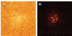
Speckle imaging has been applied to astronomical imaging and blood-flow mapping, for example, since the early 1960s. By understanding the spatial and temporal behavior of coherent light that has interacted with a scattering medium and had its "speckle" or interference pattern imaged onto a photodetector, the properties of the medium itself can be better understood. Although adaptive optics (AO) have proven superior in providing a direct image of scattering media, speckle imaging is enjoying a resurgence because of the commercial availability of highly sensitive electron-multiplying charge-coupled device (EMCCD) sensors that have photon-counting capabilities equivalent to modern CCDs, and no longer suffer from the pixel "dead-time defect" that made bright speckles look dimmer.
As Southern Connecticut State University (New Haven, CT) astronomer Elliott Horch demonstrates through images of a 12th magnitude star, speckle features that are not easily seen with a commercially available back-thinned CCD are readily observed by an EMCCD with comparable quantum efficiency at high electron-multiplying gain because this multiplication increases the signal level above the read noise. And unlike many AO systems that are optimized for use in the infrared region, speckle imaging is easily performed at visible wavelengths. Horch adds that speckle-based EMCCD imaging is now being used at the Southern Astrophysical Research and Gemini South telescopes in Chile, the Special Astrophysical Observatory 6 m telescope in Russia, and the Gemini North and Discovery Channel Telescope in the U.S. Reference: E. Horch, "Turning on to speckle imaging," SPIE Newsroom (Jun. 24, 2016); doi:10.1117/2.1201606.006584.

Gail Overton | Senior Editor (2004-2020)
Gail has more than 30 years of engineering, marketing, product management, and editorial experience in the photonics and optical communications industry. Before joining the staff at Laser Focus World in 2004, she held many product management and product marketing roles in the fiber-optics industry, most notably at Hughes (El Segundo, CA), GTE Labs (Waltham, MA), Corning (Corning, NY), Photon Kinetics (Beaverton, OR), and Newport Corporation (Irvine, CA). During her marketing career, Gail published articles in WDM Solutions and Sensors magazine and traveled internationally to conduct product and sales training. Gail received her BS degree in physics, with an emphasis in optics, from San Diego State University in San Diego, CA in May 1986.