FOCAL-PLANE ARRAYS: Geiger-mode focal plane arrays enable SWIR 3D imaging
MARK ITZLER and MARK ENTWISTLE
One of the most dramatic transformations taking place in the field of imaging is the growing prevalence of three-dimensional (3D) imagery. The display of 3D imagery is emerging as an indispensable tool in medical settings and industrial applications, is becoming commonplace in the movie industry, and is poised to experience explosive growth in consumer electronic gaming. This proliferation of 3D image display has been accompanied by significant advances in the complementary task of 3D image capture. Various techniques for recording 3D images have been in use for some time (such as the application of stereography using 2D images of a scene obtained from different angles); perhaps the most effective approach for 3-D image capture is light detection and ranging (lidar). Using lidar techniques, short optical pulses illuminate a scene and precise time-of-flight measurements of the pulse reflections from objects in the scene enable accurate distance information that provides the third spatial dimension normally absent when images are recorded using ambient reflected light. Construction of a 3D camera is then accomplished by independently applying the lidar technique to every pixel of an imaging focal plane array (see Fig. 1).
For many imaging applications (especially those related to defense), there are strong drivers for lidar imaging in the shortwave infrared (SWIR) region of the optical spectrum: the availability of high-performance, short-pulse laser sources in this wavelength band (Nd:YAG at 1.06 μm and erbium-doped fiber lasers at 1.55 μm); the covertness of these sources, since they are not visible to widely proliferated night-vision goggles; low-loss atmospheric propagation at these wavelengths; and, for wavelengths beyond 1.4 μm, their relative eye-safety when compared to shorter wavelength sources.
Single-photon lidar
The ultimate sensitivity for optical imagers is obtained by efficiently detecting just a single photon at each imaging pixel. For 3D lidar imaging, it is also imperative that single-photon detection is fast and temporally precise since distance precision will be determined by time-of-flight measurement accuracy.
One detector technology capable of providing single-photon detection at SWIR wavelengths with excellent timing accuracy is the avalanche photodiode (APD) based on the indium-gallium-arsenide-phosphide (InGaAsP) material system. When this device is biased above its avalanche breakdown voltage, the absorption of just a single photon can lead to a macroscopic avalanche current pulse that is easily detected by backend electronic circuitry. For appropriately designed APDs, this mode of operation—often referred to as the Geiger mode—provides efficient, temporally accurate single-photon detection. In addition, these detectors can be readily integrated into large-format arrays with high pixel density. By hybridizing Geiger-mode APD (GmAPD) detector arrays to suitable CMOS readout integrated circuits (ROICs), we have developed a GmAPD focal plane array (FPA) that serves as an ideal sensor engine for 3D imaging lidar systems with single-photon sensitivity at SWIR wavelengths.
Because these GmAPD FPAs can create lidar images with much lower pulse energies than systems that use conventional detectors and tend to require return pulses of at least dozens or even hundreds of photons per pixel for reliable detection, this GmAPD performance advantage translates to greatly reduced system-level size, weight, and power requirements. It also enables new capabilities, such as pioneering work at MIT Lincoln Laboratory (Lexington, MA) demonstrating effective 3D imaging through dense foliage.1
These GmAPD FPA-based cameras also have the potential to disrupt existing high-performance 3D imaging applications such as aerial mapping in which a single detector is mechanically scanned to build up 3D image data sets. Scanning of a single detector currently limits key metrics of 3D mapping applications such as data acquisition rate and data point density on the ground. In fact, 3D imaging will inevitably follow a technology evolution similar to that of IR imaging techniques by migrating from single scanned detectors to large area (2D) formats approaching millions of pixels per imager.
GmAPD FPA design and performance
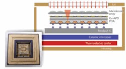
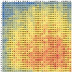
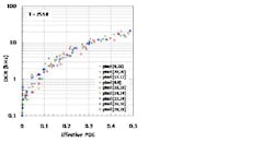
The heart of our FPA is a chip stack consisting of a GmAPD detector array flip-chip bonded to a CMOS ROIC with a gallium phosphide (GaP) microlenslet array attached to the back surface of the detector array to provide high optical fill factor (see Fig. 2). Pseudorandom counters embedded in every pixel of the ROIC provide pixel-level time-of-flight timestamps when reflected lidar pulses are detected. Pulse returns as weak as a single photon are efficiently detected using GmAPDs as the active elements of each pixel. ROICs with very fast readout times of approximately 3 μs enable the rapid collection of a large number of imaging frames. With a typical "range gate" on the order of 2 μs during which the FPA is armed to sense lidar pulse returns, these sensors can achieve frame rates approaching 200 kHz. An integrated thermoelectric cooler (TEC) maintains chip operating temperatures approximately 50°C below ambient temperature, and hermetic packaging provides stable operation in harsh environments.For 3D imaging at 1.55 μm, we have produced FPAs with equivalently high yield providing 100% pixel operability. The detection of these longer-wavelength photons imposes a moderate compromise in performance in the form of higher DCR since a narrower-bandgap semiconductor must be used to efficiently absorb these less energetic photons.
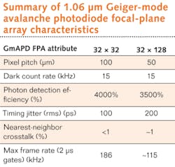
The temporal accuracy with which a photon arrival can be detected, referred to as timing jitter, is important because it limits the precision of distance measurements. For our 32 × 32 FPAs, we have demonstrated a root-mean-squared timing jitter as low as 100 ps.
With a 13 bit counter in each pixel, the time-stamp data output from the entire FPA running at its most rapid frame rate generates a very high-rate data stream of 4 Gbit/s. The transfer of this data from the ROIC to our FPGA-driven board electronics is accomplished using a 32 channel data bus. Subsequent data transmission to a computer or other storage medium can be accommodated using a dual-connector Camera Link interface configuration. A turnkey camera module currently incorporates separate 3.75 in. boards for FPA control, FPGA electronics, and other support electronics.
Additional operating modes and future developments
The digital nature of the GmAPD avalanche response dictates that it is not sensitive to the number of photons arriving at the detector. However, the probability of detection increases dramatically with the number of photons in a return pulse. For example, at operating conditions for which the probability of detecting a single-photon input is approximately 25%, the probability of detecting an input pulse consisting of 10 photons is >95%.4 This is an impressively high detection probability for an amount of radiation (about 10 photons) that is below the sensitivity threshold of most existing imaging technologies.
Although the operation of our existing camera electronics is intended for generating 3D image data, it is also possible to use this sensor to acquire 2D passive images with single-photon sensitivity by collecting ambient radiation. More complex active/passive imaging techniques can then be enabled by combining these two imaging modalities.A key focus for future developments beyond the current 32 × 32 FPA products is increased pixel count and decreased pixel pitch. We have already demonstrated prototype FPAs using four times as many pixels in a 32 × 128 format with half the pitch, at 50 μm (see table). The GmAPD FPA designs and processes demonstrated to date provide an excellent platform for realizing even larger formats (MIT Lincoln Laboratory has demonstrated arrays as large as 64 × 256 with 50 μm pitch), as well as the migration to pixel pitch of less than 50 μm. In the meantime, the 32 × 32 GmAPD FPA sensors will aid the development of a new generation of 3D imaging systems based on lidar techniques.
REFERENCES
1. B.F. Aull et al., "Three-dimensional imaging with arrays of Geiger-mode avalanche photodiodes," Proc. SPIE, 5353, 105-116 (2004).
2. M.A. Itzler et al., J. Mod. Opt., 54, 2-3, 283-304 (2007).
3. M.A. Itzler et al., "Design and performance of single photon APD focal plane arrays for 3D LADAR imaging," Proc. SPIE, 7780, 77801M (2010).
4. M.A. Itzler et al., "Geiger-mode avalanche photodiode focal plane arrays for three-dimensional imaging LADAR," Proc. SPIE, 7808, 78080C (2010).
Mark Itzler is CTO and Mark Entwistle is hardware design manager at Princeton Lightwave, 2555 US Route 130 S., Cranbury, NJ 08512; e-mail: [email protected]; www.princetonlightwave.com.


