COLIN COATES and CHRIS CAMPILLO
In scientific cameras, the choice between electron multiplying charge-coupled device (EMCCD), interline CCD, and CMOS sensor technologies has involved tradeoffs between speed, field of view, noise, dynamic range, and pixel resolution, not to mention cost. Recent advances in scientific CMOS (sCMOS) cameras, however, have eliminated the primary performance tradeoffs by simultaneously delivering unprecedented speed, ultralow noise, high dynamic range, and a large field of view, while remaining affordably within the "workhorse camera" price category. As a result, sCMOS cameras are poised to capture many of the existing interline CCD and some of the EMCCD applications. The unique properties of interline CCD and EMCCD sensors do mean, however, that they are still preferred in certain niches, such as those involving long staring times or single molecule detection.
A history of tradeoffs
The most important parameters that define the performance limits of a scientific-grade digital camera are: dark current—measured in e-/pixel/second; read noise—measured in e-/pixel; speed—defined in frames per second (frames/s) or megapixels per second (Mpixels/s); field of view—a function of pixel size and the total number of pixels; quantum efficiency (QE)—the probability of a photon being detected as signal at a given wavelength, expressed as percent; and dynamic range—the ratio of the largest measurable signal to the smallest detectable signal. Until now, no available sensor technology could optimize all these parameters simultaneously, so camera choice has been based on the sensor that delivered the best compromise for the particular application. This tradeoff has been particularly problematic for biologists who need high speed to image biochemical events in real time but often simultaneously require low noise, high resolution and a large field of view (that is, a large number of pixels).
Low-noise CCDs
Charge-coupled devices have long been considered the ultimate imaging sensors because of their ability to provide very low noise and high QE. This includes dark current much lower than 1 e-/pixel/s, readily achieved when the camera is cooled to below -30°C, even down to -100°C in high-end CCD cameras. Read noise of several electrons per pixel used to be a limiting issue for some low-light/high-speed applications, but this was successfully addressed by development of the EMCCD. Here the signal from each pixel is boosted by several stages of on-chip amplification before reaching the readout electronics. This effectively reduces the readout noise by a factor equal to the signal amplification.
The critical limitation of CCDs has been speed. Every column of pixels must be serially moved to the readout register and then transferred to the common readout node. With just a 1k × 1k pixel sensor, that's a million pixels to be processed in this way. Faster readout electronics can be used, but these increase noise. Binning groups of pixels or using only a subset of the entire chip also offers higher speed but sacrifices resolution and field of view.
An interline architecture offers some improvement to CCD frame rate. Here, each column contains a charge storage area blocked to incoming light so it can be read out while the exposed pixels are acquiring the next frame. Similar 100% duty cycles can be achieved with frame-transfer CCDs (the architecture also used in EMCCDs) that have a masked storage area to which the entire frame is transferred for readout. All of these schemes, however still involve a limited number of common readout ports (usually one), imposing a severe restriction on frame rate.
CMOS limitations
A different type of sensor is the CMOS chip that's based on the same complementary metal-oxide semiconductor technology used in electronic integrated circuits. With a reputation for lower cost and relatively poor performance, CMOS imagers are widely used in consumer devices like cell phone cameras. In the sense that they are semiconductor devices with photosensitive areas in each pixel that convert incident photons into electrons, CMOS image sensors are similar to CCDs. However, unlike a CCD—which serially transfers each pixel's charge to a common output structure—each pixel of a CMOS device contains its own circuitry for charge-to-voltage conversion and signal buffering. Hence a CMOS array is characterized by intensely parallel readout.
Despite this speed advantage, CMOS technology has not dominated scientific digital imaging because of its inferior performance in other areas, including higher read noise, higher dark current, inferior pixel-to-pixel uniformity, limited dynamic range, and lower QE. Furthermore, CMOS chips tend to have a higher number of defects than do CCDs—generally in the form of "hot" pixels with high dark noise. Some array manufacturers developed a hybrid technology with a CMOS sensor bump-bonded onto a CCD backplane, which resulted in cameras with speeds as high as 50 full frames/s and a noise floor of a few electrons. For many applications, this noise was still too high and the technology is expensive.
Scientific CMOS
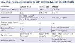
Most recently, advances in semiconductor and MEMS technologies, as well as the fast signal-processing capabilities of a field-programmable gate array (FPGA), have enabled the performance limitations of CMOS devices to be addressed by use of appropriate hardware and firmware, thereby opening up the technology to scientific applications. At Andor we have built a next-generation scientific camera based on CMOS without any of the noted performance limitations. The Neo sCMOS camera delivers the high-speed benefits of CMOS (up to 100 Hz full frame), with ultralow noise, high QE, wide dynamic range, high resolution, and a large field of view (see table).
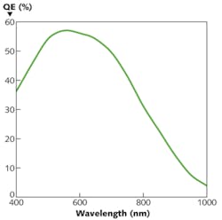
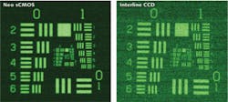
How has this been achieved? The low QE of earlier CMOS devices is a direct result of pixel complexity. With several transistors in each pixel, the area of each pixel available for photodetection is well below 100%. The new sCMOS sensor uses physically smaller transistors and related features, as well as a micro-lenslet array for light concentration, resulting in a fill factor similar to CCDs and a QE of 57% (see Fig. 1). Even more important, this is the first camera technology to offer read noise of only 1 electron without amplification (see Fig. 2). This is achieved at a rate of 30 full frames/s (or 200 Mpixels/s). Even at 100 frames/s, the read noise is only 1.4 e-, a number that is generally unachievable by CCD cameras, even when operated at 1 Mpixel/s or slower.As previously mentioned, defects in CMOS usually take the form of hot pixels with higher dark noise. To counter this, vacuum cooling to -40°C of the new sCMOS camera removes almost all of these defects. Consequently, nearly every pixel delivers dark current of 0.03 e-/ pixel/s, which is markedly better than earlier CMOS cameras. Furthermore, as a result of Andor's experience with EMCCD technology, it was recognized that there is a need to actively deal with the occasional spurious high-read-noise pixel in order to obtain the perfect low-light images that biologists prefer. This optional filter works by having the FPGA identify any spurious isolated pixel and replace its value with the mean of its nearest neighbors. This is programmed to correct where the spurious read noise is relatively high (5–6 e-) and only under low-light situations. The camera's FPGA also flat-field corrects the entire sCMOS sensor output, compensating for the fixed differences in pixel response caused by the natural variations in on-pixel signal processing characteristic of CMOS chips. As a result, fixed pattern noise is completely eliminated.
Applications—A shifted balance
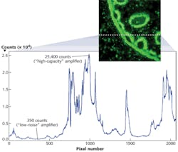
The performance advances inherent to the new generation sCMOS camera have significantly shifted the balance between sCMOS, CCD, and EMCCD technologies. As noted, the new sCMOS cameras provide speed and field of view without compromising other parameters, but they are also very flexible. Their large dynamic range, for instance, means they work well in both ultralow-light and medium-light applications. Also, their region of interest can be readily altered, enabling the camera to be used as a lower-resolution device. So sCMOS cameras may become the first choice for many applications—including scientific—where the imaging parameters vary from experiment to experiment.
However, both the other technologies will continue to have important application niches. For example, the "zero noise" characteristics of well-optimized EMCCDs are still necessary for extremely low-light applications such as single molecule detection or single photon counting. And while interline CCDs will suffer most in terms of lost applications, their superior dark current means they will still be preferred for long exposure (several minutes) applications, such as chemiluminescent gel blots for DNA/RNA sequencing and for in vivo luminescence imaging of animals. Furthermore, interline CCDs will likely maintain a notable near-term cost advantage.
Colin Coates is product manager for imaging cameras and Chris Campillo is sales engineer for US West Coast at Andor Technology, Belfast, Northern Ireland; e-mail [email protected]; www.andor.com.


