HYPERSPECTRAL IMAGING: One-shot camera obtains simultaneous hyperspectral data
Commercially available spectral imaging systems capture the intensity information from a scene and display it as a digital image (with x and y spatial coordinates), while also gathering the spectral information for every pixel or row of pixels in the scene. Multispectral systems generally obtain information in a few discrete spectral bands, while hyperspectral imaging systems obtain spectral data over a much broader, continuous wavelength range. The resultant three-dimensional "data cube" is built up using sequential data capture in which point-scanning, line-scanning, or filter-based methods gather the spectral and spatial information over time as an event unfolds. Unfortunately, this method is incapable of capturing phenomena that change on a time scale faster than the acquisition speed of the detectors being used. And even though simultaneous methods exist, they are typically very expensive as they require the use of multiple cameras or multiple detector/multiple filter systems firing at the same time.
Recognizing the need for lower-cost, high-performance simultaneous image capture for fast-moving events such as explosions (or even for some biological events monitored through fluorophore excitation), scientists at Horiba Scientific (Edison, NJ) in partnership with Snapshot Spectra (Pasadena, CA) have developed a patented, one-shot simultaneous hyperspectral imaging (SHI) camera that simultaneously captures spatial information and its corresponding spectral information over the wavelength range from 400 to 850 nm.
One-shot, simultaneous image capture
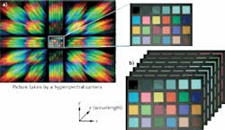
To obtain simultaneous hyperspectral information in a one-shot single measurement step, the SHI camera relies on a two-dimensional transmission dispersive element sandwiched between a pair of imaging lenses. The first or input lens collimates the light coming from the scene of interest and the second lens re-images the diffracted light from the dispersive element (between the two lenses) onto the sensor. The uniqueness of the system is based on the dispersive element design that creates a 2D diffraction pattern at the sensor (see figure). The image projected on the sensor is an accurate representation of the field of view in the center of the image (undiffracted zero order) and higher diffracted orders around the center. Since the angle of diffraction is a function of the wavelength, with the angle increasing from short (blue) to long (red) wavelengths, the higher-order diffracted images are essentially "smeared" wavelengths across the sensor containing all the spectral information in the scene. The hypercube is then generated from a software reconstruction algorithm using the raw image data as input.
The robust design has no moving parts and can be applied to hazardous environments. Furthermore, the technique can use different dispersive elements and sensors to optimize resolution, sensitivity, and detection speed to suit the application of interest. "This technology enables spectral imaging applications that were not possible with currently available technologies, especially ones with transient or dynamic scences," says Francis Ndi, applications scientist at Horiba Scientific. "Its rugged and portable design also makes it possible to do such measurements in varied and harsh environments such as industrial as well as field work—given that it does not need a computer for acquisition."

Gail Overton | Senior Editor (2004-2020)
Gail has more than 30 years of engineering, marketing, product management, and editorial experience in the photonics and optical communications industry. Before joining the staff at Laser Focus World in 2004, she held many product management and product marketing roles in the fiber-optics industry, most notably at Hughes (El Segundo, CA), GTE Labs (Waltham, MA), Corning (Corning, NY), Photon Kinetics (Beaverton, OR), and Newport Corporation (Irvine, CA). During her marketing career, Gail published articles in WDM Solutions and Sensors magazine and traveled internationally to conduct product and sales training. Gail received her BS degree in physics, with an emphasis in optics, from San Diego State University in San Diego, CA in May 1986.
