Ge nanowire photodetector integrated on Si has high photoconductive gain

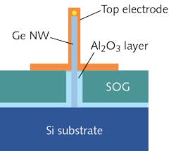
On-chip optical interconnects require both emitting and detecting components—the smaller, the better. Researchers at the University of Michigan (Ann Arbor, MI) have developed a germanium nanowire (Ge NW) photodetector for operation at a 1.55 μm wavelength with a diameter of only 20 nm integrated on a silicon (Si) substrate. The single-nanowire detector, which sticks up perpendicularly from the wafer, has a photoconductive gain of 2000 and a responsivity of 22.6 A/W. The fabrication process is CMOS-compatible.
The photodetector is made up of the Ge nanowire partially embedded in a layer of spin-on-glass (SOG) on a Si substrate, with a thin film of aluminum oxide (Al2O3) separating the nanowire from the SOG. A thin-film top electrode coats the projecting portion of the nanowire. To test the device, light from a continuous-wave laser with a maximum output of 0.8 W was focused to a 300 μm radius and passed through the Si (which is transparent at 1.55 μm). The photocurrent was linear with respect to optical power without saturation up to 800 mW. The researchers note that the photocurrent can be further increased by creating a number of nanowires connected in parallel as a single detector. Reference: U. Otuonye et al., Appl. Phys. Lett., 110 (2017); http://dx.doi.org/10.1063/1.4982648.

John Wallace | Senior Technical Editor (1998-2022)
John Wallace was with Laser Focus World for nearly 25 years, retiring in late June 2022. He obtained a bachelor's degree in mechanical engineering and physics at Rutgers University and a master's in optical engineering at the University of Rochester. Before becoming an editor, John worked as an engineer at RCA, Exxon, Eastman Kodak, and GCA Corporation.