Photonics Applied: Terahertz Imaging: Terahertz imaging tackles solar cell and semiconductor process inspection
Optoelectronic systems for terahertz spectroscopy and imaging have matured significantly over the last decade. An important driver of this trend is the increased use of integrated optical technology from the telecom sector, enabling the buildup of compact and high-performance time-domain spectroscopy (TDS) systems.
In modern terahertz TDS systems, fiber-coupled and integrated components have fully replaced distributed free-space beam optics. This not only implies advantages in terms of space requirements, but also facilitates the integration of terahertz measurement capabilities into different kinds of system environments for scientific and industrial applications. Specifically, wafer analysis systems can use terahertz microprobes for high-resolution near-field imaging.
The TeraFlash system from Toptica Photonics (Munich, Germany) is a fiber-based terahertz TDS module with optical and electronic integration at a high level.1, 2 Almost every component—including a femtosecond pulsed laser, optical time-delay components, and data acquisition and control units—is housed in a 19 in. rack-mountable box. The only external components are two fiber-coupled photoconductive (PC) antennas used for the generation and detection of terahertz radiation by optical excitation from the TDS module.
Commercial integration
The optical fiber/cable connection between the external terahertz antenna components and the TDS system brings terahertz testing into new application environments, thanks to a small footprint and vast freedom from radio-frequency (RF) signal interference.
Operating at 1550 nm, our terahertz system combines Toptica's TDS module with our PC near-field probes, minimizing signal dispersion in the optical fiber and keeping the duration of the applied optical sampling pulses below 100 fs. The resultant terahertz system can record a full terahertz time-domain transient in only 20 ms, which is a great advantage for applications requiring many sequential terahertz measurements such as inline quality inspection, non-destructive testing, and raster-scanning-based terahertz (near-field) imaging.
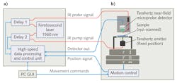
In contrast to the standard configuration for free-space transmission measurements of a sample wherein the terahertz radiation generated by the emitter antenna is collimated and focused onto a far-field detector antenna, our fiber-based terahertz TDS system combines the TeraFlash source module with the Protemics TeraCube near-field scanning system that includes a PC near-field probe (the Protemics TeraSpike TD-800-X-HR-WT) for terahertz detection and imaging (see Fig. 1).3
A computer unit controls the TDS module as well as the near-field imaging system. During measurements, the motion control unit of the raster scanning system transmits the current position of the sample continuously to the data acquisition unit, where it is combined with the terahertz data recorded at each position. The high sampling rate of the TDS module enables surface-scanning operation under continuous movement (without stop-and-go interruptions) for full terahertz transient detection.
The PC near-field probe consists of a 1-μm-thin low-temperature-grown gallium arsenide (GaAs) cantilever featuring a pair of tapered electrodes that form the PC switch at the tip of the probe. It records the transmitted terahertz field close to the sample surface. In contrast to electrooptic crystals as near-field probes, it is characterized by lower invasiveness and higher sensitivity.
Scattering-tip-based probes can only record z-fields and aperture-based probes only in horizontal (x, y) fields. In contrast, our PC near-field detectors are designed to be selectively sensitive to field vector components in x-, y-, or z-directions.
Scientific applications
With a maximum spatial resolution of 3 to 10 μm when hovering only a few microns above the surface of a sample under test, new applications in industry and science are now possible with the Protemics terahertz imager.
In the scientific sector, for example, researchers at the Dutch Institute for Fundamental Energy Research (DIFFER; Eindhoven, Netherlands) found that resonance frequencies of metamaterials observed at far-field distances can differ significantly from the ones monitored in the near-field range.4 Their research showed values of 0.62 THz at 1 μm distances vs. 0.85 THz in far-field distances (around 24 cm).
For future sensing applications of such structures, it is therefore very important to have direct access to the near-field properties that determine the sensor/analyte interaction properties. Also, coupling mechanisms between closely spaced resonant structures—giving rise to electromagnetically induced transparency—can be monitored directly at the interacting structures.5 In one example, it was demonstrated that electromagnetically induced transparency in metamaterials can be enhanced to an absolute value >80% by tuning the long-range coupling states of periodic metamaterials to the individual resonance frequencies of the involved metamolecules.
Industrial wafer analysis
Besides scientific applications, industrial analysis is increasingly relevant for terahertz imaging systems. For example, the contact-free determination of material properties such as sheet resistance values (Rsh) or other charge-carrier-related properties of semiconductor wafers and solar cells can be retrieved from the transmitted terahertz signal by the application of analytic model descriptions. For example, the Tinkham formula is commonly used for sheet resistance extraction from terahertz transmission data obtained at thin (<10 μm) conducting layers on semi-isolating substrates.6
So far, contact-free measurements of sheet resistance distributions with up to micron-scale resolution are not possible over full wafer-scale areas. Such capabilities are, however, required to effectively optimize the fabrication processes of microstructures on solar cells through direct inspection in an early stage of production instead of doing cumbersome tests on fully processed cell series afterwards.
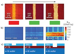
In one example, the formation of high-efficiency cell contacts by etching-paste-induced silicon-nitride (SiNx) layer removal is of particular interest.7 There, an etch paste is used to open the SiNx. To find the optimal etching end-point, the opening of the SiNx is monitored in dependence to the curing temperature of the paste by terahertz near-field transmission imaging. The goal is to fully remove the SiNx layer and leave the diffusion layer below the contacts mostly unaffected regarding sheet resistance. While the visual control can provide information about the completeness of the SiNx removal process, it cannot give information about the remaining quality of the diffusion layer.
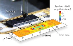
The terahertz transmission images, however, can clearly reveal when the opening of the SiNx is completed and the etching of the diffusion layer has started. Even small (still acceptable) damages to p+ diffusion layers caused by over-etching can be detected that are not recognizable through visual control or other contactless Rsh imaging methods—the latter because of resolution constraints (see Fig. 2). More importantly, the terahertz scanning method is not influenced by the surface morphology of the dielectric layer, but only by the diffusion below it. Now, the optimal end-point of the etching process can be reliably found in a very early stage using the Protemics modular terahertz imaging system.The near-field measurement data reveals the emission and the propagation of a terahertz wave along the surface of the DUT that allows identification and localization of device failures such as scattering centers of the propagating terahertz pulse with a lateral resolution of a few microns (see https://goo.gl/aajUyv).
To identify these scattering centers, the terahertz wave is monitored as it is generated from a femtosecond laser pulse at the center of the chip and propagates as a spherical wave towards the edges. When parts of the propagating pulse hit the edge of the chip, the wave is reflected, leading to a clearly resolved interference pattern (see Fig. 3). Note that the entire process occurs within 40 ps and the lateral resolution of the image is 20 μm.
The new generation of terahertz time-domain spectroscopy modules have the best prerequisites for implementation in a variety of system environments such as in our near-field imaging systems. Together with application-specific terahertz devices such as micron-scale resolution probes, as well as task-oriented data analysis, terahertz imaging sensors will become an increasingly important tool in contact-free quality inspection and non-destructive testing of solar and semiconductor wafer components.
REFERENCES
1. See https://goo.gl/6FvPCW.
2. N. Vieweg et al., J. Infrared Millim. THz Waves, 35, 10, 823–832 (Oct. 2014).
3. See https://goo.gl/pgj4gN.
4. A. Bhattacharya et al., Phys. Rev. B, 93, 035438 (2016).
5. A. Halpin et al., Phys. Rev. B, 96, 085110 (2017).
6. P. Spinelli et al., Energy Procedia, 92, 218–224 (2016).
7. P. Spinelli et al., "High resolution THz scanning for optimization of dielectric layer opening process on doped Si surfaces," IEEE 44th Photovoltaic Specialist Conference (PVSC), Washington, DC (2017).
Michael Nagel | CEO, Protemics
Michael Nagel is CEO at Protemics (Aachen, Germany).
Björn Globisch | Head, Terahertz Sensor Systems Group at the Fraunhofer Institute for Telecommunications
Björn Globisch is Professor for Physics at the Technical University Berlin and head of the Terahertz Sensors and Systems research group at the Fraunhofer Institute for Telecommunications (Fraunhofer HHI; Berlin, Germany).
Simon Sawallich | Chief Research Officer, Protemics
Simon Sawallich is chief research officer at Protemics (Aachen, Germany).


