CMOS Sensors: Graphene and quantum dots combine for broadband CMOS camera
Although photonic silicon integrated circuits (ICs) on complementary metal-oxide semiconductor (CMOS) electronic platforms have made 100 Mpixel imaging sensors possible, the integration of nonsilicon semiconductor components with CMOS architectures has been difficult, limiting imaging sensors to visible wavelengths. But a collaboration between researchers at ICFO, ICREA, and the Barcelona Institute of Science and Technology (all in Barcelona, Spain), and Graphenea (Donostia-San Sebastian, Spain), has removed these limitations by successfully integrating a two-dimensional (2D) material—graphene—with quantum-dot (QD) photodetectors on a CMOS platform to create a broadband (300-2000 nm) imaging sensor.1
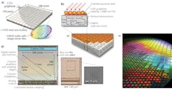
The 388 × 288 array (approximately 110,000) graphene-QD photodetector channels are monolithically integrated and connect to the individual electronic components of a CMOS readout integrated circuit (ROIC), enabling a digital camera with sensitivity from visible through shortwave-infrared (SWIR) regions.
Back-end-of-line CVD graphene
Starting with a conventional CMOS die with ROIC components, each pixel of the CMOS sensor is covered with a layer of graphene fabricated using a chemical vapor deposition (CVD) process. After patterning the graphene to define a pixel shape and connecting it to the underlayer ROIC via vertical metal interconnects, a layer of lead sulfide (PbS) colloidal QDs is deposited on top of the graphene layer in a spin-casting process (see figure).
This back-end-of-line process—which takes place after the initial CMOS process and includes metalization, interconnect, and dielectric layer deposition—creates an image-sensor sandwich that brings light onto the PbS QDs and transfers photogenerated electron holes to the graphene where they are transmitted as a signal to the ROIC and processed as a standard change in the conductance of the graphene transport layer. But unlike standard silicon-based pixels, the QD-graphene pixel sandwich is sensitive to wavelengths beyond the standard visible realm of silicon.
The CVD graphene offers a high mobility (around 1000 cm2/Vs), enabling an ultrahigh gain of approximately 108 and responsivity greater than 107 A/W—performance levels that are from 10,000 to 100,000X higher than QD-only photodetectors. The sensor noise is significantly less in graphene than in high-quality silicon, further improving performance with high detector sensitivity, broad wavelength range (that can be tailored using different QD materials), and 0.1–1.0 ms switching times.
Although the frame rate in the prototype sensor is limited to 50 frames/s with 211 mW power consumption, alternative ROIC designs could improve imaging speeds to a few-hundred frames per second as determined by the carrier lifetime in the QDs.
Imaging experiments on subjects under a variety of illumination schemes confirmed exemplary performance of the image sensor, even without manufacturing optimization. More than 95% of the pixels can see light with 10-7 W/cm2 intensity values—roughly corresponding to partial-moon and twilight conditions.
ICREA professor Gerasimos Konstantatos says, "Having such a broadband photodetector covering the visible and the SWIR is not essential only for imaging, but also for spectroscopy. Although our prototype image sensor has not reached the sensitivity of InGaAs [indium gallium arsenide] costly counterparts, we expect to get there by designing and optimizing the ROIC, as well as improving further the properties of graphene on CMOS."
ICREA professor Frank Koppens adds, "In general, graphene-CMOS imaging technology will enable a vast amount of applications ranging from low-cost pocket and smartphone cameras, fire control systems, passive night vision and night-surveillance cameras, automotive sensor systems, medical imaging, food and pharmaceutical inspection, and environmental monitoring, to name a few."
REFERENCE
1. S. Goossens et al., Nature Photon. online (May 29, 2017); doi:10.1038/nphoton.2017.75.

Gail Overton | Senior Editor (2004-2020)
Gail has more than 30 years of engineering, marketing, product management, and editorial experience in the photonics and optical communications industry. Before joining the staff at Laser Focus World in 2004, she held many product management and product marketing roles in the fiber-optics industry, most notably at Hughes (El Segundo, CA), GTE Labs (Waltham, MA), Corning (Corning, NY), Photon Kinetics (Beaverton, OR), and Newport Corporation (Irvine, CA). During her marketing career, Gail published articles in WDM Solutions and Sensors magazine and traveled internationally to conduct product and sales training. Gail received her BS degree in physics, with an emphasis in optics, from San Diego State University in San Diego, CA in May 1986.
