DAN CROFT
Engineers designing imaging systems for low-light environments recognize the importance of the image sensor to the overall ability of the system to capture images with high quality. New sensor alternatives make it necessary to fully understand the trade-offs when choosing an image-sensor solution. A range of complementary metal-oxide semiconductor (CMOS) image sensors now challenges traditional charge-coupled-device (CCD) sensors.
To choose the best sensor for cameras and systems that must produce high-quality images under low-light conditions, system designers must evaluate several characteristics that affect not only image quality but also system complexity and cost. The primary attributes of a sensor that determine its ability to capture images under low-light conditions include dark current, dynamic range, noise, fill factor, color sensitivity imbalance, and device integration, as well as device and related system costs.
Image-sensor characteristics
Image sensors capture photons and convert them into electrical signals that are subsequently processed into images for storage, transmittal, analysis, or printing. The ability of a sensor to capture images in low-light environments is critical in applications such as security, biometrics, and consumer imaging. General-purpose sensors with attributes that enhance low-light sensitivity are ideal for these applications.
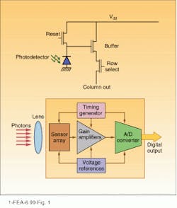
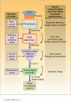
A pixel, the fundamental element of an image sensor, consists of several components. A pixel in a typical CMOS device includes a photodiode that produces a charge proportional to the incident light, plus transistors that provide buffering, switching, and reset functions (see Fig. 1). The raw signal for the image being viewed is formed when charge from the pixel capacitor is sampled, buffered, and transferred to amplifiers and analog-to-digital converters (ADCs). These functions can all be integrated into the sensor. The flow diagram of a typical signal through a CMOS image sensor highlights sources of noise and key sensor characteristics (see Fig. 2). To capture details in a low-light environment, a sensor must separate minute differences in the signals generated by the exposed pixels. The ability of a sensor to accurately differentiate between the wide range of light intensities contained in most scenes is a major determinant of the fidelity of the resulting images.Dark current and quantum efficiency
For a sensor to be useful in low-light applications, the part of each pixel that captures and measures the incident photons and converts them into an electronic charge must be of high quality—this is a critical requirement. Two measures of this quality in a pixel are the dark current and quantum efficiency.
In an ideal sensor, the dark current—the amount of current discharging the photodiode in the absence of incident light—would be zero. In practice, however, it is not. Because the photodiode in the pixel acts as a capacitor with a discharge rate proportional to the incident light, the dark current can slowly discharge the capacitor to a voltage that would also be produced at a low level of incident light. When this happens, the rest of the system will be unable to determine whether the pixel actually "sees" something or has just obtained a charge level from the dark current. Basically, the dark current establishes one component of the "noise level" of pixel output.
To design a system that can distinguish the subtle differences between dimly lit objects and absolutely dark objects, it is important to choose an image sensor with low dark current—the lower the better, within the overall constraints of the system design. Typical dark-current values for CMOS and CCD sensors range from 0.075 nA/cm2 to well above 2.0 nA/cm2. And highly optimized CCD sensors can extend this range down to 0.010 nA/cm2.
The quantum efficiency of an image sensor is a measure of the proportion of the incoming photons that are converted into electrons, which subsequently discharge the pixel capacitor. Pixel capacitance is typically extremely small, so that a relatively few converted electrons result in a detectable change in the voltage on the capacitor. When a pixel is fully charged (full exposure), its peak output voltage might only be 1.0 to 1.3 V.
Signal-to-noise ratio
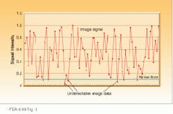
The signal-to-noise ratio (S/N) of a sensor, specified in decibels (dB), is critical if low-level signals are to remain detectable. For low-light applications where subtle differences in light levels must be captured, less than 1 mV of noise on a chip can be perceived as graininess in the image. A high noise floor can quickly overwhelm the low-level signals generated in low-light or shaded conditions (see Fig. 3). The output of the sensor pixels is digitized by an ADC via an amplifier. One or more ADCs may be fabricated on-chip with the pixels to form an integrated image sensor device.The dynamic range of the ADC may differ from the S/N of the pixel array. These two specifications are sometimes confused because both are expressed in decibels. Even when pixel dynamic range is high, the dynamic range of the image sensor device may be limited by the resolution of the ADC(s). Today, general-purpose sensors usually have an 8-bit ADC, which yields a dynamic range of 48 dB; a 10-bit ADC, which gives a dynamic range of 60 dB; or a 12-bit ADC, which produces a 72-dB dynamic range.
Pixel size and fill ratio
The ability to capture low-light images is also determined by the size of the active (light-gathering) area of each pixel. With integrated-sensor designs, the pixel typically contains multiple transistors in addition to the active photo diode area. Transistor size is limited for a given silicon-manufacturing process, but overall pixel size can be varied. The ratio of the active area to the total area (active area plus support electronics area) is the "fill factor," which is expressed in percent.
Sensor designers have several choices when designing an image array and the associated pixels. Larger pixels enable the sensor to capture more photons for improved pixel dynamic range. But larger pixels also utilize more silicon area, which drives up the device-manufacturing cost. The size of the active area can be set to optimize three factors—low-light sensitivity, overall sensor size, and the size of the optics necessary to project the desired image over the entire array.
Instead of increasing the active area, some sensor manufacturers add extra steps to the manufacturing process to apply a microlens over each pixel. A microlens captures most of the incident light and focuses it onto the active area, which increases the effective fill ratio. Here the trade-off is between the added cost of the microlens processing steps and the cost of the larger active areas. Typically, a pixel with a microlens requires a narrower incident light angle than a pixel that does not use a microlens, which has design implications for the lens of the camera.
Color sensitivity imbalance
Device designers who produce sensors for capturing color images have an interesting challenge because different color pixels exhibit varying sensitivity to different frequencies of incident light. A sensor that is more sensitive to red light than blue light, for instance, creates an imbalance in the captured image. The imbalance can be corrected digitally after the ADC step, but at that point the imbalance has already added to ADC quantization noise.
A more sophisticated technique is available, however, in which color-specific gain control or amplification can be applied to the output of the pixel before the signal is digitized by the ADC. Without color-specific gain control, a sensor at a given exposure setting will not be able to utilize the full range of the ADC, and noise will be amplified by postprocessing in channels that exhibit lower-than-average sensitivity. With color-specific gain control, an image sensor makes the full range of the ADC(s) available for each color, independent of pixel sensitivity. In turn, this allows a design engineer to utilize the full dynamic range of the ADC.
Enhanced functionality
Cost issues must be carefully studied to select the best image sensor for a low-light application. Besides the cost of the sensor itself, one must consider the impact of the sensor on the rest of the system. Various trade-offs must be evaluated, such as the effect of integration within the sensor device.
Typical CMOS sensors incorporate more functional integration than do CCD sensors, which are manufactured by a specialized process, thereby making it a challenge to add image-processing circuitry to the chip. In contrast, CMOS sensors are made with the same high-volume processes used to build most computer chips, so digital circuitry can be added to enhance sensor functionality.
The CMOS sensor chips typically integrate pixel array, timing logic, sampling circuits, amplifiers, reference voltage supplies, and ADCs. However, CCD sensors require a minimum of two support chips to accomplish the same functions. The increased integration offered by CMOS sensors can reduce system complexity, reduce manufacturing costs, and allow smaller camera designs.
Also, because analog functions are included on the CMOS sensor device, sensor designers have additional options with CMOS, such as "tuning" the analog signal path to optimize image quality or providing a completely digital interface. Practical considerations limit the functions that can be added to a CMOS sensor chip, however. Extra circuitry increases die size and, therefore, raises device cost. More circuits also increase the possibility that noise from one section of the chip will interfere with the operations of another section. For instance, noise generated by the digital portion of the chip can interfere with highly sensitive front-end analog circuits and degrade image quality, unless sensor designers minimize the impact of that noise. Also, the additional circuitry produces heat that, if not properly managed, can reduce image quality.
Achieving high-quality images
To maximize the quality of the image produced by a camera, the design engineer must consider sensor quality, in combination with other elements of the camera—specifically the lens, the image-processing pipeline, and any image-compression method used. These elements can contribute significantly to poor image quality by introducing image noise and other artifacts into the system. A camera with a sub-par lens, image-processing, or image-compression function—even if equipped with a highly sensitive sensor—will produce an image of less-than-optimum quality.
CCD sensors have traditionally had better image quality than CMOS image sensors. However, that situation is changing for several applications in which the latest CMOS-based sensors match the low-light performance of general-purpose CCD devices. For applications in which high-quality images must be produced in low-ambient-light environments, a high-quality, highly integrated CMOS sensor offers overall system advantages.
Dan Croft is senior product manager for imaging devices in the Hewlett-Packard Components Group, 1000 NE Circle Blvd., Corvallis, OR 97330; [email protected].


