John C. Carson, David R. Shostak, and David E. Ludwig
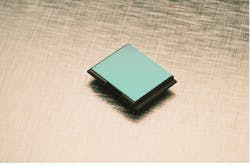
Stacked, thinned-silicon integrated circuits (ICs) provide the densest possible concentration of electronics circuitry for signal-processing or computational applications. Dubbed 3-D Silicon, the stacked chips can be integrated with imaging detector arrays to create "smart sensors" for visible and infrared applications. Because the technology also has use in ultrahigh-density mass digital storage systems for data recorders, digital signal processors, and computers, the economies of scale associated with these applications will pave the way for stacked-chip sensors to move into the commercial market (see Fig. 1).
Imaging sensors typically include an m ¥ n detector array integrated monolithically, or by hybrid means, with read-out electronics that buffer and multiplex the individual detector signals. In conventional systems, signals are serially transmitted to display or processing systems. As imaging sensor applications have evolved, it has become increasingly desirable to integrate signal-processing capabilities in the sensor, with functions ranging from response-nonuniformity correction and digitization to spatial-temporal filtering and ultimately to biological levels of recognition. 3-D Silicon is a method for achieving these goals.
Integrated smart-sensor focal-plane assembly
Smart-sensor designs are centered around highly parallel processing, stopping short of providing a separate channel for each pixel. Typically, a signal-processing channel will handle 50 to 100 pixels of the detector array; designers trade affordability, determined by the number of chips in the stack, with the level of parallel processing desired.
In the chip shown, a signal-processing channel handling 100 pixels applies 10 to 20 bits of nonuniformity correction to each pixel. Each preprocessor chip in the stack incorporates 256 such channels, with each operating at a frame rate of 100 Hz. The chips output a digitized signal with 8- to 12-bit precision. The detector array size determines the number of these chips in the stack; a 512 ¥ 512 array requires 10 chips. Additional chips are typically included for data compression in industry-standard JPEG (still photography) or MPEG (motion picture) formats. Memory elements can also be included.
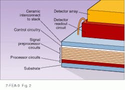
The recent capability to stack heterogeneous chips and multiple chips and chip types per layer has been a breakthrough in 3-D Silicon technology. These layers are referred to as Neo-Chips (Irvine Sensors, Costa Mesa, CA) because they look and perform like standard ICs but are composed of multiple, diverse dies. Thus standard imaging detector arrays can be integrated with elements ranging from microprocessors and digitizers to memory units and data-compression chips (see Fig. 2). A typical chip might contain 256 Mbit of flash memory plus the related control and buffer electronics.
The technology allows the stack dimensions to substantially exceed typical IC sizes, permitting integration with large-format imaging devices ranging from 20 to 35 mm in diameter. Because more dies can be included in the stack, the chips can perform higher-level and more-intensively parallel processing. The architecture also provides interconnection paths at any point between layers in the stack. Conventional architectures permit interconnects only along the perimeter of the stack, limiting the number of possible connections. By allowing die connections throughout the whole area of the chip, the new technology can potentially accommodate thousands of pin-outs.
Video imaging
Focal-plane arrays for visible imaging are generally charge-coupled-device (CCD) detectors, monolithic devices ranging from 200 to 4000 pixels on a side. Digital photography is a common application of this technology. Detector technology is relatively mature, so these applications require minimal correction for signal nonuniformity or outage. Instead, processing elements digitize images, compress them using JPEG, MPEG, or wavelet algorithms, and store them in nonvolatile memory.
With inherent low power dissipation and compact, highly favorable form factors, or configurations, stacked-chip technology is an efficient solution for visible imaging. The approach eliminates unwanted and costly circuit-board requirements. Short, highly parallel interconnects greatly reduce capacitive and inductive parasitics, leading to reduced power requirements in comparison with conventional systems.
Stacked sensors can also provide scene-based image motion compensation, correcting for operator hand jitter, vehicle motion, or platform vibration by detecting motion of features in the scene and reformatting the output image. A new IC, the inner product convolution engine, performs motion correction, data compression, and pattern recognition. Developed by Irvine Sensors, this device performs multiplication and addition operations at the rate of 16 billion operations per second while consuming less than 30 mW of power.
Infrared imaging
Military infrared imaging systems have continuously pushed toward higher resolutions. At present, focal-plane arrays offering resolution of 256 ¥ 256 pixels are common in the field. Programs underway to produce the next generation of detectors are expected to reach formats larger than 1024 ¥ 1024 on single hybrid assemblies.
Even as resolution increases, conflicting requirements to reduce size, weight, and power while maintaining narrow bandwidth and low cost are major constraints inhibiting the deployment of these next-generation systems. Traditionally, to achieve such goals existing circuits are redesigned to provide compact, lightweight, higher-density wafer architectures. This approach has several pitfalls, however. The need for state-of-the-art wafer technology drives cost and constrains designs. Because each design is unique, any circuit change requires extensive reinvestment of nonrecurring engineering. Finally, the capability and design of a system is limited to what can be achieved in a series of two-dimensional (2-D) circuit and board layouts. Folded 2-D assemblies require exotic connector and cable designs, and system reliability and cost become driven by cables and boards.
The stacked-chip approach circumvents these pitfalls. Typical of the type of configurations possible is a sensor assembly currently undergoing integration and test at Irvine Sensors that incorporates a commercially available 160 ¥ 120 indium antimonide detector and readout hybrid topping a stack of four integrated circuits. Each custom IC contains 80 channels of analog-to-digital conversion, gain correction, and offset correction; a channel supports 60 pixels of the detector array. Gain and offset coefficients are stored in 40 kbit of on-chip SRAM. Overall, the sensor focal-plane array consumes 125 mW when operating at a 60-Hz frame rate at a temperature of 80 K.
The stacked-sensor approach simplifies functions previously difficult to perform under any conditions; good examples are large-format configurations operating at moderate to high framing rates. Power and bandwidth limitations were major impediments to conventional implementation of such sensors, but the stacked-sensor approach makes them feasible.
Consider a 1024 ¥ 1024 array operating at 100 Hz. The design requires the basic readout to support an analog output data rate greater than 125 MHz. Driving analog signals of about 2.5 V across a cable at these frequencies requires significant power consumption, and the heat generated by dissipation of that power exceeds normal cryogenic cooling capabilities. In addition, to achieve 12-bit resolution, the signal preprocessor and processor would need to handle digitized data at roughly 1.5 Gbit/s. Signal-processor boards for this amount of data are large, expensive, and power-hungry.
With 3-D Silicon technology and the image-processor circuits developed at Irvine Sensors, the same configuration array as above was realized with digital data output at 1 V. The output data rate was reduced to 60 MHz, while offering the same resolution as above. Reduced data rate and signal levels minimize power consumption. Noise immunity is a direct benefit of the design. Because the processing units are integrated with the detector and mounted inside the cooling unit, the output data stream is digitized within the Dewar, circumventing thermal corruption of analog data. The reduced number of components, connectors, and cables increases system reliability, and, because the signal path across high inductance/capacitance cables is reduced, power requirements are reduced. Finally, the stacked sensor is lightweight and compact. o
ACKNOWLEDGMENTS
The first circuits to link standard IR detector arrays to nonuniform connectors and digitizers were developed under the ARPA Flexible Manufacturing Program in support of Northrop Grumman Corporation (Los Angeles, CA). Neo-Chip technology is first being demonstrated under an SBIR contract with NASA Jet Propulsion Laboratory (Pasadena, CA) using their active-pixel sensor technology. Scene-based image motion compensation has been demonstrated under an SBIR with NASA Marshall Space Flight Center (Huntsville, AL). The inner product convolution engine was first demonstrated under the Silicon Neuron Seeker Program for the Ballistic Missile Defense Organization.
FIGURE 1. Stacked sensor performs image detection and signal processing in a compact, lightweight device with low power requirements.
FIGURE 2. Sensor chi¥integrates detector array with image-processing and control circuitry. Functions include signal preprocessing (analog-to-digital conversion and nonuniformity correction), and processing (data compression and formatting) operations. Blue segments are ceramic interconnects to the chi¥stack.

