Infrared LASERS
Optically pumped antimonide device lases at 4 microns
Chris Chinnock
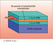
Researchers at the University of Houston`s Space Vacuum Epitaxy Center (SVEC, Houston, TX) working with the Naval Research Laboratory (NRL, Washington, DC) have reported development of a mid-IR semiconductor device that lases near room temperature. The device is fabricated from InAs/GaInSb/InAs/AlGaSb in a quantum-well structure (see figure). The device is optically pumped by a Nd:YAG laser at 1.06 µm and a Ho:YAG laser at 2.06 µm. Laser operation was demonstrated up to 285 K, which, according to the research team, is the highest-temperature operation yet achieved with a mid-IR semiconductor laser.
Led by Shin-Shem Steven Pei, SVEC`s associate director of research, the team demonstrated laser operation near 4 µm, with output powers of 650 mW at 81 K and 200 mW at 170 K. The device stops lasing above 285 K, which, Pei believes, is due primarily to internal heating. To address this problem, SVEC is working with the NRL to redesign the laser structure. Results so far are encouraging, and Pei sees no "showstoppers" en route to his goal of a thermoelectrically (TE) cooled laser in one or two years. Achieving efficient 1-W operation at room temperature will take some doing, however. The key, as suggested by R. Q. Yang of SVEC, is to modify the structure to incorporate the concept of a cascade laser.
Cascade lasers were first demonstrated about two years ago by researchers at AT&T Bell Laboratories (Murray Hill, NJ; see Laser Focus World, June 1994, p. 15). Such lasers do not create photons in the laser cavity by the recombination of electron-hole pairs, explains Pei. Instead, they are unipolar devices, creating photons with either holes or electrons. What`s more, as an electron cascades down the energy steps in the structure, additional photons are created at each step, achieving a multiplicative effect. The result is that the devices can be highly efficient.
Cascade lasers have another benefit--the output wavelength can be determined during fabrication. Instead of the wavelength being determined mostly by the bandgap of the materials, which is the case with the current design, the output wavelength of cascade structures can be altered by adjusting the thickness of individual layers.
The mid-IR band (3-5 µm) is particularly important because it is one of the atmospheric windows with min imal water absorption. In addition, many chemicals, molecules, and compounds have strong absorption lines in this band.
Limited options
Current mid-IR sources have shortcomings. The most popular option today, for example, is to pass the output of a solid-state laser through an optical parametric oscillator to convert the energy to the desired mid-IR wavelength. Such devices are large and costly. Alternatively, lead-salt diode lasers are available, but they are also expensive and require cryogenic cooling.
Because of the limited source options, many systems perform trace-element sensing with near-IR instead of mid-IR lasers. Pei believes that if a room-temperature semiconductor laser can deliver about 1 W in the mid-IR, then room-temperature thermal detectors also can be used. This would eliminate the bulky cryogenically cooled detectors now used to achieve sensitivity. "A room-temperature source and detector make a very powerful combination that will enable a wide variety of portable applications," he says. SVEC is now seeking more agency and commercial support to further development of this new type of laser.
CHRIS CHINNOCK is a technical writer based in Norwalk, CT 06850
Fabricated from InAs/GaInSb/InAs/AlGaSb, a semiconductor structure provides output in the 3-5-µm region at temperatures as high as 285 K.
