AVALANCHE PHOTODIODES: Silicon photomultipliers expand uses for Geiger-mode APD technology
Silicon photomultipliers—arrays of parallel interconnected avalanche photodiodes (APDs) in Geiger mode—offer high dynamic range and linearity by using a structure of multiple microcells with a common anode, allowing multiple photons to be detected (and counted) within the same timeframe.
CHRISTOPH WITTE and PHILIPPE BÉRARD
In recent years, many papers and articles have been published about silicon photomultipliers (SiPMs) and their ability to replace photomultiplier tubes (PMTs) in applications like positron emission tomography (PET), high-energy physics, and radiation detection, as well as analytical instrumentation.1-2 These SiPMs are basically arrays of parallel interconnected avalanche photodiodes (APDs) operated in a voltage range above the breakdown voltage. This mode of operation is named "Geiger mode" and the voltage applied above breakdown is usually referred to as overvoltage.
Through implementation of a structure of multiple microcells with a common anode, developers have achieved a significant increase in the dynamic range and hence linearity of single-photon-counting detectors over a large active area by allowing multiple photons to be detected (and counted) within the same timeframe. The main critical performance parameters of SiPMs are high photon detection efficiency, low dark noise, low crosstalk and afterpulsing, and fast timing resolution.
Performance metrics
The most important performance parameter of almost any detector is photon detection efficiency (PDE), describing the probability of an incident photon creating a detectable current flow (or pulse) at the detector output stage. On the SiPM, PDE basically consists of three parameters: quantum efficiency (QE), which describes the probability of a photon creating a photoelectron within one microcell; avalanche probability (Pa), the probability of this photoelectron creating an electron avalanche through impact ionization, leading to a measurable current flow at the anode; and geometrical efficiency or fill factor (FF), which is the ratio between active microcell area and total microcell area, including the "dead space" between multiple microcells on a single SiPM pixel. The parameters are related through the equation PDE = QE × Pa × FF.
While the FF is mostly a geometrical parameter determined by the surface of the p-n junction in the silicon material, Pa and QE are defined by the type of material chosen ("p on n" or "n on p") and details of the structure.
On SiPMs, there is a direct tradeoff between PDE and dynamic range: As the number of microcells on a given detector area is increased (by use of smaller microcells), the percentage of dead space between those microcells will increase proportionally and thereby decrease geometrical efficiency and overall PDE. This tradeoff has to be considered based on individual application requirements.
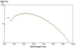
The C30742 SiPM chip from Excelitas is based on a "p on n" structure and a standard 50 × 50 μm microcell design in various chip sizes, with an overall PDE of approximately 34% @ 510 nm (peak wavelength) and a spectral bandwidth ranging from 300–950 nm at an operating voltage of 5 V above breakdown voltage. The design approach differs significantly from the design of other SiPMs that use standard complementary metal-oxide semiconductor (CMOS) manufacturing processes by allowing the creation of a deep diffused depletion region, resulting in lower capacitance and a PDE curve with significantly higher sensitivity and signal-to-noise ratio at longer wavelengths (see Fig. 1). The relatively high value of overvoltage allows the diode to work with Pa close to saturation to maximize the overall PDE.
The PDE value can be further increased in subsequent product generations (exceeding 40% at peak) by improving the geometrical efficiency through careful silicon chip layout—circumventing design tradeoff effects at the expense of other parameters such as crosstalk and dark-count rate. Another approach is to use a more complex antireflection coating that will improve the quantum efficiency below 400 nm by 10–20% at the expense of a few-percent loss at or above 500 nm.
Dark noise, or dark-count rate, is another parameter of importance for SiPMs. A "dark count" means an output pulse not created by incident photons but by (thermal) carriers within the silicon structure. The dark-count rate represents the most limiting performance factor for SiPMs in applications predominantly using traditional vacuum-tube PMTs. Due to the physical nature of silicon-based products, the dark-count rate (per area) for SiPMs is several orders of magnitude higher than for vacuum tubes and therefore complicates a simple direct substitution with solid-state products. While the higher average noise floor can typically be subtracted from the measurement data, the statistical variation of the dark-count rate (given Poisson-statistical distribution, defined as the square root of the average dark-count rate) cannot be subtracted and therefore limits the minimum detectable signal of the SiPM.
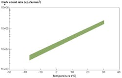
Based on our proprietary low-noise APD technology, the new Excelitas C30742 SiPM structure provides a dark-count rate of much less than 200 kcps (thousand counts per second) per square millimeter at room temperature (see Fig. 2). This performance was achieved by designing a detector with a low k-factor, or electron-hole ionization ratio, which is a well-known characteristic of low-noise APDs operated in the linear region.
Other important factors to be mentioned for SiPM performance are crosstalk and afterpulsing, both of which are troublesome for linearity and operation of the device at higher overvoltage. Crosstalk is mainly caused by photons (or electrons) emitted by the silicon structure of an activated microcell, causing another avalanche in an adjacent microcell. While this effect cannot be observed in single-pixel APDs (due to the lack of neighboring cells), it must be carefully controlled on the SiPM so it will not compromise linearity and dynamic range of the sensor.
The most effective way to avoid (optical) crosstalk is the design of photon-absorbing trenches to incorporate photon-absorbing structures (either vertical or v-shaped trenches) between the microcells on the SiPM chip. We use v-shaped trenches on four sides of each microcell to minimize optical crosstalk of the detector.
Afterpulsing is a similar effect where trapped electrons within the SiPM structure cause secondary avalanches that cannot be distinguished from real pulses created from incident photons at the output stage. Because purity of the silicon and geometry or size of the SiPM structure and the quench resistor are key design contributors to minimize afterpulsing, we used a large quenching resistor of 1 MΩ in the Excelitas SiPM design by doping polysilicon to limit the re-ignition of a microcell during its recharge.
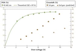
The first generation of the C30742 SiPM will be specified with total crosstalk and afterpulsing in the 10–20% range, while the next generation of chips is expected to show crosstalk in the 5–15% range (depending on design variations on the chip) at the specified operating voltage of 5 V above breakdown (see Fig. 3).
The last critical performance parameter for SiPMs is timing resolution, defined as the jitter (statistical variation) of the rise time of a pulse caused by incident photons. Silicon photomultipliers can generally be described as fast photon detectors, having both a fast rise time in the nanosecond range as well as a small jitter, or timing resolution.
While timing-resolution-optimized designs at least partially conflict with designs optimized for other parameters, our SiPM can be operated at a high overvoltage (beyond the optimum recommended 5 V if an optimal timing resolution is required) with an electrical field that comes very close to the detector surface. This ensures high mobility and small traveling distance of the charge carrier, and overall it minimizes the timing jitter. This high tolerance to overvoltage means that arrays of SiPM devices can be setup with all devices operating at the same voltage (even though each chip has a slightly different breakdown voltage). This also means that individual diodes do not need digital-to-analog or "DAC tuning" of operation voltage, simplifying the electronics design and minimizing weight and power consumption of the SiPM array enclosure.
SiPM applications focus
The main application driving SiPM development for high-volume OEM business is PET, where solid-state solutions like APDs have already started to replace PMTs in recent years. The biggest advantage over PMTs certainly being their extremely high immunity to electromagnetic fields, APDs and SiPMs allow a combination of PET imaging with magnetic resonance imaging (MRI), enabling truly simultaneous acquisition of high-resolution anatomical and functional images.3
Positron emission tomography requires a precise coincidence measurement of two high-energy photons emitted in an almost exact 180° angle from each other. As the high-energy photons create a fairly large number of visible photons within a short timeframe through a scintillator such as lutetium yttrium orthosilicate (LYSO) before being detected, a generally higher dark-count rate (compared to PMTs) is acceptable. The challenge is to precisely measure the exact timing of the very first incident photons on both sides of the detector ring to confirm true coincidences; hence, the principal critical parameters are a good timing resolution (in the range of 200 ps or less) and high PDE. Furthermore, the application requires dense packaging of the chips to allow an optimal coverage of the detection area with active pixels.
Similar performance requirements can be postulated for high-energy physics applications like Cherenkov telescopes, used in imaging the very short flash of Cherenkov radiation generated by the cascade of subatomic particles produced when, for example, a high-energy gamma ray strikes the atmosphere; and in calorimeters, an experimental apparatus used in particle physics that measures the energy of subatomic particles. Very high PDE at the wavelength range of interest is required, from ultraviolet (UV) well into the visible region.4
While timing resolution in most cases is not a critical performance parameter, the applications do call for high dynamic range, good linearity, and low dark-count rates at ambient temperatures to avoid early saturation during the measurements. For instance, in both previously mentioned applications, the number of photons emitted will be proportional to the initial gamma energy, which can vary by several orders of magnitude.
As outlined previously, there is a direct tradeoff between PDE and dynamic range based on the number and size of microcells on the active area (dynamic range is also influenced by other factors such as individual dead time of microcells) that needs to be factored into the choice of the most suitable SiPM design. The ability to densely package the devices to cover an optimal detection area with active pixels is also considered a crucial factor. While in calorimeters, radiation hardness becomes an additional performance requirement due to the huge energy and charged-particle flow created during the particle physics experiments. Other environmental considerations such as minimizing failure rates and downtime come into play for large-area telescope installations located in remote regions.
Introducing SiPMs in analytical instrumentation is not as straightforward as in the aforementioned cases; PET is a coincidence measurement mostly dependent on detector timing resolution, and high-energy physics measurements are typically looking for events creating millions of photons. Both of these applications can therefore tolerate fairly high dark-count rates, as compared to PMTs. However, the requirement to measure random emission of low-light levels in analytical instruments adds low dark counts to the set of detector requirements. The typical wavelength of emitted light is shifted to the green-to-near-infrared (NIR) range, whereas most scintillator applications require high sensitivity in the UV-to-blue wavelength range. Furthermore, system manufacturers would rather use a modular plug-and-play type of detector vs. packaged chips only. Our response to these requirements is the Excelitas LynX SiPM module (see Fig. 4).
Silicon photomultipliers continue to develop and are becoming increasingly popular in low-light-level photon counting and similar applications. Both PET and Cherenkov radiation detection are likely early volume adopters of this technology, but specific scientific and analytical applications will no doubt take off in due course. The SiPM technology is developing and, while not mature, is already able to offer stable and repeatable performance suitable for industrial and medical uses, through adoption of suitable manufacturing processes.
REFERENCES
1. A.G. Stewart et al., IEEE J. Quantum Electron., 44, 2, 157–164 (2008).
2. B. Dolgoshein et al., IEEE Trans. on Nuclear Sci., 53, 2, 636–640 (April 2006).
3. D. Henseler et al., "SiPM Performance in PET Applications: An Experimental and Theoretical Analysis," IEEE Nuclear Science Symposium and Medical Imaging Conference (NSS/MIC), Orlando, FL (2009).
4. P. Bérard et al., "Performance measurement for a new low dark count UV-SiPM," IEEE NSS/MIC, Valencia, Spain (2011).
Christoph Witte is product manager, low light level detection, Excelitas Technologies GmbH, Wenzel-Jaksch-Strasse 31, D-65199 Wiesbaden, Germany. Philippe Bérard is a member of technical staff, R&D for silicon photomultipliers at Excelitas Canada, 22001 Dumberry Rd, Vaudreuil-Dorion, Quebec J7V 8P7, Canada. E-mail: [email protected]; www.excelitas.com


