PHOTONIC FRONTIERS: ROOM-TEMPERATURE IR IMAGING: Microbolometer arrays enable uncooled infrared camera

Photon detectors are the ultimate in speed and sensitivity in the thermal or longwave infrared (LWIR), the band of wavelengths from about 7.5 to 14 μm where room-temperature objects have peak blackbody emission. But combining that ultimate sensitivity with low noise to give high image quality requires cooling the detectors and the cameras that contain them to temperatures where they don't emit blackbody photons in the band they are trying to detect. That makes direct photon detection too costly and cumbersome for many potential applications.
An attractive alternative for such LWIR applications is detecting the absorption or radiant heat rather than photons. Radiant heat sensors, called bolometers, have long been used for IR measurements. Now arrays of many thermally isolated microbolometers can record images in the thermal IR. Crucially, microbolometers do not require cooling, so this reduces their cost, size, and complexity. Steady improvements in sensitivity, array size, and production technology are making uncooled IR cameras practical and affordable for applications ranging from searching for enemy troops to watching the sides of a dark road for deer that might dart into the path of a vehicle.
Microbolometer basics
The earliest practical bolometer, invented in 1878, measured heat by detecting temperature-induced changes in the electrical resistance of an IR-absorbing material. A Wheatstone bridge circuit measured heat absorption by comparing the resistance of one piece of the material that absorbed IR light to the resistance of a matching piece of the same material that was kept in the dark.
Modern microbolometers measure temperature changes caused by IR absorption in individual pixels, which are thermally isolated and assembled into focal-plane arrays (FPAs). Originally developed in the 1970s, microbolometer arrays were classified until the early 1990s because of their importance for military night-vision systems. The technology has now found civilian as well as military applications, but many microbolometer arrays remain subject to Unite States export controls, and some technical details remain sensitive.
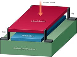
Each pixel in an array is a very low-mass IR-absorbing structure supported by thin legs, which limit heat conduction to the underlying substrate, as shown in Fig. 1. The lower the mass of the illuminated pixel, the less IR energy is needed to increase its temperature a given amount, and the more sensitive it is. The arrays often are called MEMS (microelectromechanical system) devices, although they don't move in operation.
Two classes of IR-absorbing materials are used in microbolometers. Pyroelectric or ferroelectric crystals generate electrical signals that are directly proportional to the temperature increase caused by IR absorption; the most common material now in use is barium-strontium titanate. Other materials act as thermistors, in which the electrical resistance changes with temperature. As in the original 19th century bolometer, measuring the resistance of a microbolometer pixel measures the incident IR intensity. The leading materials today are the semiconductors amorphous silicon and vanadium oxide (often abbreviated VOx), which are compatible with the standard semiconductor processing technology used to fabricate the read-out circuits that generate images.1
Several factors influence microbolometer performance. The sensitivity depends on how much the resistance or other electrical signal changes with temperature, and this depends on the absorbing material. The pixel response time also is important; absorbers should collect heat quickly and hold it long enough for measurement, then dissipate it before the next frame is recorded. A typical rule of thumb is that the time response should be no longer than one-third of the interval per frame, about 10 ms for a 3 Hz frame rate. Response time and performance also depend on the read-out integrated circuit (ROIC), which collects temperature data from all pixels for each frame. Noise usually is measured as noise-equivalent temperature difference (NETD), with lower being better, and 50 mK a desirable target.
Trends in focal-plane arrays
Microbolometer arrays have followed the same trends as other FPAs, with individual elements shrinking and the number of pixels increasing. Early microbolometer arrays had small pixel counts and center-to-center spacing of 50 m. Spacing of 25 μm is now standard, and 17 μm arrays are now in production, says Charles Hanson, principal of the consulting firm SenseIR (Richardson, TX). Although some arrays on the market have as few as 160 × 120 pixels, most now range from 320 × 240 pixels to 1024 × 768 pixels, with 640 × 480 pixels the most popular size. Arrays with closer spacing and multi-megapixel counts have been demonstrated.
Most microbolometer absorbers today are either VOx or amorphous silicon. Both semiconductors act as thermistors, and can be deposited on silicon with modern chip-processing techniques. The two materials have similar spectral response, but each has its advantages and its corporate advocates.
Developers are increasing pixel counts as they shrink pixel spacing. At the 2011 SPIE Defense, Security + Sensing (DSS) Symposium, Stephen Black of Raytheon Vision Systems (Goleta, CA) said the company was developing 2048 × 1536-element, 17-μm VOx arrays for DARPA's Tailwind program, which seeks 3-Mpixel LWIR detector arrays for unmanned aerial surveillance craft.2 Raytheon also is working on arrays made of sub-17-μm elements. Black will give an update on the multi-megapixel array and other work at this year's SPIE DSS in April.
ULIS (Veurey Voroize, France) has developed 17 μm arrays with up to 1024 × 768 pixels of amorphous silicon. In 2011 the company reported a 640 × 480 pixel array with NETD of 45 mK and a thermal time constant of 9 ms, allowing operation at frame rates to 60 Hz with power consumption of only 150 mW.3 Both time constant and NETD are in the range sought for practical applications.
New materials and methods
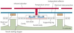
Developers are looking to new materials and fabrication techniques to reduce cost and expand the range of applications. Fabrication of MEMS elements directly on CMOS read-out circuits now requires amorphous materials for the IR-absorbing material. To avoid that limit, the Microsystem Technology Lab at the KTH Royal Institute of Technology (Stockholm, Sweden) fabricates separate MEMS and CMOS wafers, then bonds them together. That allows growth of single-crystal heat-sensitive absorbers of Si/SiGe quantum-well materials with pixels spacing as small as 17 μm.4 Audun Roer of Sensonar Technologies AS (Horten, Norway) has used a similar technique to make a 384 × 288 pixel Si/SiGe quantum-well array with 25 μm spacing5, and will describe more details at SPIE DSS this month.Mitsubishi Electric (Amagasaki, Hyogo, Japan) is taking a different approach, using single-crystal silicon-on-insulator (SOI) pn diodes as temperature sensors rather than amorphous semiconductors. They started with single-diode sensors, but last year reported that using matched pairs of diodes allowed them to reach NETD of 21 mK and thermal time constant of 16 ms in a 25 μm, 640 × 480-element array.6 At this month's SPIE meeting, Daisuke (Takamuro) Fujisawa and colleagues will describe making a 2000 × 1000-element array with 15 μm pixels, which can be read at a 30 Hz frame rate. Although its NETD is higher at 84 mK, the thermal time constant improved to 12 ms.
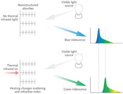
The General Electrical Global Research Center (Niskayuna, NY) has made a radically new type of absorbing element: adding single-walled carbon nanotubes to nanostructures in the scales of butterfly wings. When light illuminates the tropical Morpho butterflies, scattering and interference within the nanostructures generate complex iridescent patterns. The same structures can "serve as low thermal mass optical resonators," write Andrew Pris and colleagues in Nature Photonics.7 Adding carbon nanotubes to the nanostructures caused them to absorb midwave IR (MWIR) at 3 to 8 μm, heating the nanostructures and changing their refractive index. That affects how the nanostructures scatter visible light, so observing changes in light scattering could be used to measure IR illumination, as shown in Fig. 3. "The new thermal detection platform described here overcomes the limitations of existing bolometer approaches, with their complex physical and thermal pixel design, and makes possible the previously unavailable capabilities of high sensitivity and fast speed, without the need for thermoelectric cooling, in a heat-sink-free operation," they write.Applications outlook
Thermal imaging cameras have a host of potential applications that go far beyond traditional military night-vision systems. Firefighters and emergency crews can use them to identify hot spots or people in empty buildings. Energy auditors can use them to spot leaks or poorly insulated areas. They could be used in a wide range of medical and industrial applications to map temperatures. They can even be mounted in cars, to improve the safety of night driving by spotting hazards beyond the range of headlights, such as a deer that might bound into the road.
The limiting factor for most of these applications is cost. Handheld thermal imaging cameras with 320 × 240-pixel resolution are readily available on the Internet, but buying one will set you back about $7500. That can be a literal lifesaver for a busy fire department, but it's a showstopper for many other applications. The microbolometer array is a key factor in that price, and the more new technology can bring those prices down, the more applications will be possible.
REFERENCES
1. C. Hanson, "Amorphous-silicon bolometers could surpass IR focal-plane technologies," Laser Focus World, 47, 4, 67–71 (April 2011).
2. S.H. Black et al., "Uncooled Detector Development at Raytheon," Proc. SPIE, 8012, 80121A (2011); doi:10.1117/12.887816.
3. J.-L. Tissot et al., "High-performance uncooled amorphous silicon video graphics array and extended graphics array infrared focal plane arrays with 17-μm pixel pitch," Opt. Eng., 50, 6, 061006 (June 2011).
4. F. Forsberg et al., "High-performance infrared micro-bolometer arrays manufactured using very large scale heterogeneous integration," presented at 2011 Intl. Conf.on Optical MEMS and Nanophotonics (OMN), pp. 9–10 (Aug. 8–11, 2011).
5. A. Roer et al., "High performance LWIR microbolometer with Si/SiGe Quantum well thermistor and wafer level packaging," Proc. SPIE, 8185, 818507-1 (2011).
6. D. Takamuro et al., "Development of new SOI diode structure for beyond 17 μm pixel pitch SOI diode uncooled IRFPAs," Proc. SPIE, 8012, 80121E (2011); doi:10.1117/12.884556.
7. A.D. Pris et al., "Towards high-speed imaging of infrared photons with bio-inspired nanoarchitectures," Nat. Photon., advanced online publication (Feb. 12, 2012); doi:10.1038/NPHOTON.2011.355.

Jeff Hecht | Contributing Editor
Jeff Hecht is a regular contributing editor to Laser Focus World and has been covering the laser industry for 35 years. A prolific book author, Jeff's published works include “Understanding Fiber Optics,” “Understanding Lasers,” “The Laser Guidebook,” and “Beam Weapons: The Next Arms Race.” He also has written books on the histories of lasers and fiber optics, including “City of Light: The Story of Fiber Optics,” and “Beam: The Race to Make the Laser.” Find out more at jeffhecht.com.

