3D CMOS time-of-flight imager uses new photodiode design

Three-dimensional CMOS time-of-flight sensors operate by determining the distance of different portions of a scene based on the delay recorded by individual pixels in a sensor co-located with a modulated, diffuse illumination source. To operate at distances of several meters, short nanosecond-scale pulse lengths are needed with short integration times for the photogenerated charges, presenting such challenges as short transit time, low noise, and fast readout for each pixel. To address these challenges, researchers at the Fraunhofer Institute for Microelectronic Circuits and Systems (IMS; Duiburg, Germany) developed a new intrinsic lateral-drift-field photodiode (LDPD) that achieves a 30 ns complete charge transfer from the pixels into the readout node and accumulates charge over many readout cycles to lower the signal-to-noise ratio.
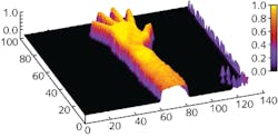
The LDPD is fabricated in a 0.35 μm CMOS process, and owes its functionality to a surface-pinned, nonuniformly n-doped well that induces an intrinsic lateral-drift field parallel to the detector surface in the direction of the pixel-readout node, effectively funneling the photogenerated charges to a specified node for almost noiseless reset and readout. The 40 μm2 pixels (38% fill factor) were assembled into a 128 × 96 pixel sensor and a human arm was easily imaged in 3D using the sensor within a standard camera setup in conjunction with a 905 nm pulsed source (with a pulse duration of 30 ns) operated at 10 kHz. Responsivity of the LDPD was 230 μV/W/m2 and dynamic range was about 60 dB. Contact Werner Brockherde at[email protected].

Gail Overton | Senior Editor (2004-2020)
Gail has more than 30 years of engineering, marketing, product management, and editorial experience in the photonics and optical communications industry. Before joining the staff at Laser Focus World in 2004, she held many product management and product marketing roles in the fiber-optics industry, most notably at Hughes (El Segundo, CA), GTE Labs (Waltham, MA), Corning (Corning, NY), Photon Kinetics (Beaverton, OR), and Newport Corporation (Irvine, CA). During her marketing career, Gail published articles in WDM Solutions and Sensors magazine and traveled internationally to conduct product and sales training. Gail received her BS degree in physics, with an emphasis in optics, from San Diego State University in San Diego, CA in May 1986.