High-speed image capture for motion analysis is used in a wide variety of applications, including vehicle-impact testing (VIT); biomechanical research; range, aerospace, and ballistics (RAB); and particle-image velocimetry. Various technologies have been developed for high-speed imaging over the years, including high-speed analog and digital video imagers using CCD senors, but until recently the high-speed film camera has been the workhorse in industrial and military applications in which both high frame rates and excellent image quality are critical. Image quality is key in these applications, in which producing beautiful full-color slow-motion images of vehicles crashing or of bombs exploding is almost equal in importance to the business of motion analysis.
The early days
The high-speed CCD cameras of the 1990s offered great advantages over film in terms of production cost and ease of use. And, whereas high-speed film technology required chemical processing of the film and digital scanning of images for computer-based motion analysis, most high-speed CCD cameras could download images directly to computers for analysis immediately after a test. Performance of high-speed CCD imagers of this time was 640 × 480 pixels or below at 1000 frames per second, with higher frame rates available at lower resolutions. But there was a growing demand for higher resolutions, better blooming suppression, and faster shutter times that high-speed CCD cameras could not easily meet.
By 1997, Eastman Kodak Motion Analysis Systems Division (now Redlake, of the Roper Industries Imaging group) had developed a 1024 × 1024-pixel, 1000-frames/s CCD camera as part of a DARPA (the Defense Advanced Research Projects Agency; Arlington, VA) project for a holographic data-storage system. The camera had 64 channels operating at 30 MHz. As a result of the number and complexity of the output channels and the power requirements of the sensor and supporting electronics, the camera mechanical design was divided between a camera head that housed optics, sensor, and channel preamplifiers, and a half-rack-mounted chassis (to which the camera head was tethered via a short cable) for the analog-to-digital converters, power supplies, frame memory, and image-processing engine. The camera produced beautifully crisp and clean images at 1024 × 1024 pixels and 1000 frames/s, but the size and cost of the camera made it impractical for use in any of the traditional high-speed camera markets. Only a few of these cameras were produced.
The move to CMOS
High-speed camera design has now shifted to an almost exclusive use of CMOS sensors. Looking back just a few years ago, it was unclear to most that CMOS sensors were capable of the image quality needed for all but low-performance, low-cost, high-volume applications such as camera-on-a-chip designs for consumer products (see "Comment," p. 57).
So why would high-speed-camera manufacturers shift from CCD to CMOS technology to get better image quality and resolution? The answer is that CMOS sensors represent a breakthrough technology for high-speed imaging because they address most of the high-speed design requirements better than CCDs.
Typical performance of high-speed CCD cameras of a few years ago was 512 × 384 at 1000 frames/s. Current requirements are for resolutions of up to 1504 × 1128 at 1000 frames/s and 100,000 frames/s at reduced resolutions. The less complex output channels of CMOS imagers allow more channels than were practical with CCDs; CMOS sensors for high-speed applications may have from 10 to 32 or more output channels. In addition, for CMOS cameras, pixels can be read out of the output channels every clock-pulse, while CCDs typically require two to four clocks per pixel. One can see that by simply doubling the number of output channels and clocking pixels at the same rate, the pixel rate increases by a factor of four.
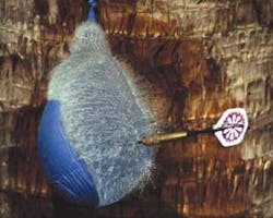
For high-speed imaging, very short exposure times are required to minimize image blur (see Fig. 1). Full-frame CCDs require a mechanical or electrical (usually liquid-crystal) shutter, both of which are limited in speed. Interline CCDs and frame-transfer CCDs use "electronic shutters," but they can suffer from image smear and are generally effective only to a minimum exposure of 20 µs. In contrast, CMOS sensors have precise electronic shuttering in the 2- to 10-µs range required for ballistics and some laboratory applications.
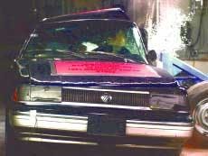
High-speed cameras often must operate in situations with very high-contrast lighting. For example, large banks of high-intensity lighting are used in VIT (see Fig. 2). Light bouncing off reflective surfaces cannot be controlled during crash testing. In RAB applications, ordnance detonations or rocket plumes are often sources of extreme contrast. But CCD sensors are prone to blooming (the overflow of electrons from one pixel to the next or to other adjacent structures). There is a tradeoff in CCDs between sensitivity and blooming suppression—but high-speed cameras require both sensitivity and blooming suppression. In contrast, CMOS sensors are not prone to blooming; while saturation effects can occur, they do not obliterate images the way blooming in CCD sensors can.
FIGURE 2. An automobile is imaged at 1000 frames/s as it undergoes a 40-mph side-impact test. The lack of blooming in the CMOS camera used in this application allows imaging under very nonuniform lighting conditions, while the camera's high light sensitivity allows automotive test engineers to scale back on expensive test illumination.
Form factor is another variable in the migration of high-speed cameras to CMOS technology. In order to fit cameras to mounts formerly used for film cameras and lower-performing high-speed CCD cameras, the newer-generation higher-performance cameras generally need to conform to the size and weight of the older products. As was seen with the CCD camera developed for the DARPA holographic data-storage system, it would be very difficult to design a high-performance high-speed CCD camera that would conform to the form-factor requirements of the traditional high-speed market.
Flexible windowing
Another important requirement for high-speed cameras is the ability to produce higher frame rates at reduced resolutions. The high-speed CCD cameras of the 1990s generally offered two to four or five resolutions. In many designs, the horizontal resolution was static and only vertical resolution could be changed. In other designs, both horizontal and vertical resolutions could be changed, but the optical center of the readout would migrate to one corner of the image. Challenges in designing CCD cameras with flexible "windowing" were apparent. In contrast, CMOS technologies allow extremely flexible readout of the sensor. This flexibility is realized in current high-speed CMOS cameras that may have thousands of selectable resolutions, helping the user to maximize performance.
Light sensitivity is a vital issue in high-speed imaging. Exposure times of 5 to 10 µs may be necessary to limit motion blur of a fast-moving projectile, especially for RAB applications, which often rely on available light outdoors. Lighting used for VIT applications is very expensive, so light sensitivity becomes a financial issue for the automotive market. Finally, light can become a heat issue for laboratory applications. Early CMOS cameras based on designs with 0.5-µm minimum feature sizes had inherent sensitivity problems. Advanced CMOS-sensor designs that use fewer components per pixel and take advantage of 0.35-µm CMOS technology provide better light sensitivity than the interline CCDs used in most of the older high-speed cameras.
The image quality of these new CMOS high-speed cameras, critically important for much of this market (and somewhat of a question as far as CMOS-sensor technology is concerned) has been very well received. Image quality of CMOS-based cameras is finding acceptance today even in the still-camera market, as evidenced by the use of sensors based on 0.35-µm CMOS technology used by Canon in some of its digital single-lens-reflex cameras.
TIM BRANDT is an applications engineer at Redlake MASD, 11633 Sorrento Valley Rd., San Diego, CA 92121; e-mail: [email protected].

