Thermal imaging on the rise
Breakthroughs in detector technology have resulted in simpler, less-expensive thermal-imaging cameras, and raised the prospects of new applications.
Outdoors, at night, a naked adult glows like a 100-W bulb, but only if viewed in the correct spectrum. Forming images from the blackbody emission from objects in our environment uses particular ranges of the infrared. The wavelengths of the radiation emitted by most terrestrial objects lie between about 3 and 12 µm. The light produced by our naked but presumably healthy friend will have a peak near 9.35 µm.
Thermal-imaging systems are distinct from "night-vision" systems that are based on image intensifiers. These systems do not detect the thermal emissions in their field of view, but rather form images from reflected moonlight and starlight. Thermal-imaging systems are also distinct from systems that image the reflected light of a near-IR source—such as a solid-state laser—to study subsurface features in medical and other applications.
The high end
The heart of any imaging system is its detector, and two principal types are used for thermal imaging—photovoltaic and thermal. Photovoltaic IR detectors produce electric current in proportion to the number of incident photons that are shorter than a threshold wavelength. Thermal detectors make use of the changes in material properties, most commonly resistance, as absorbed light heats the lattice of the detector material.
Infrared photodetectors are similar to silicon photodetectors, but use materials with bandgap energies small enough to respond to the lower-energy infrared photons, such as mercury cadmium telluride (HgCdTe, but commonly abbreviated as MCT) or platinum silicide (PtSi). Each material has its own characteristic spectral sensitivity. As with silicon photodetectors, these materials can be fabricated in detector arrays for use in the focal plane of a camera.
A major drawback to these detectors at the longer wavelengths of interest for thermal imaging is that they must be cooled to cryogenic temperatures. At room temperature, any infrared signal would be lost in the noise from thermally generated carriers in the detector material. Cooling to 193 K is required for 3- to 5-µm detectors, while 8- to 12-µm systems are cooled to the temperature of liquid nitrogen (77 K). To maintain these temperatures, the detectors are enclosed in a Dewar with a window transparent at the required IR wavelengths.
However, such photovoltaic arrays are more sensitive—by an order of magnitude or more—than thermally-based detectors. High-end imaging systems, such as those used in military applications in which accurate target recognition is a matter of life or death, bear the complexity and the cost of cryogenic cooling. Until recent years, cryogenically cooled systems were also the only choice for producing images at video rates.
Bolometric breakthrough
The other principal type of imaging sensor is the thermal detector, which measures the change in the temperature of the detector material caused by the absorption of IR light. The light energy, rather than generating electron-hole pairs, increases the lattice vibrations of the detector material. If the detector output signal is based on the resulting change in the material's resistance, the device is called a bolometer. This has become the most popular type of thermal-imaging sensor.
Thermal detectors have two significant advantages over photovoltaic types: their response is virtually flat over a very wide spectral range, and they do not require cryogenic cooling. Metallic detector materials, such as titanium, increase in resistance with increasing temperature, while semiconductor materials such as amorphous silicon, BST (barium strontium titanate), and vanadium oxide have a negative coefficient of resistance.
The response time of a thermal detector is proportional to the thickness of its absorbing material. A decade ago, this meant that bolometers could not be used in video imaging, as they took far too long to reach a new thermal equilibrium before producing a new image frame. The current revolution in thermal imaging began with the development of the uncooled microbolometer detector array by Honeywell (Freeport, IL) using techniques borrowed from silicon device fabrication.
With thicknesses of less than 1.0 µm, response times of bolometeric materials are now in the tens of milliseconds, enabling normal video operation at 30 frames/s. While less sensitive than photovoltaics, a microbolometer pixel will readily respond to a temperature change of less than 0.1°C, producing an easily detectable 1 mV. Uncooled microbolometer arrays are now commonly available in commercial imaging systems.
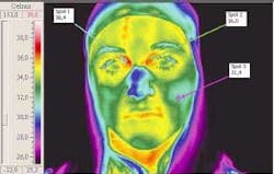
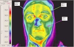
While perhaps 20 times more expensive than a standard video camera, this technology is emerging as a new tool for a wide range of applications, including security and surveillance, fire fighting, and quality inspection. In daylight, thermal systems are sometimes able to "see" through smoke and fog. Thermal-imaging systems using microbolometers are well suited for screening for individuals infected with SARS, which requires the remote sensing of the skin temperatures of large numbers of people in public places (see Fig. 1).
The typical microbolometer detector has a comparatively small number of pixels, perhaps a 160 × 128 array of 50-µm elements. While this makes for a noticeably pixilated result, the spatial resolution is sufficient for the targeted applications. Software is used to filter the digital image data, convert it to video resolution, and can also produce a false-color representation of temperature contours. Mid-format, 320 × 256 arrays with 25-µm-sized pixels are available, with larger formats (640 × 512 or 1280 × 960) under development.
Focusing on cost
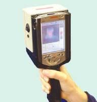
Much of the development effort however has been directed at lowering the cost of the thermal-imaging camera. Although not requiring cryogenic cooling, cameras using microbolometer arrays have needed a thermoelectric cooler (TEC) to stabilize the sensor assembly. The assembly is in a vacuum package, thermally isolated from the rest of the camera. To produce an accurate image, it must remain unaffected by radiation from the camera body itself.
Recently, cameras have become available that require no TEC stabilization, thereby reducing their complexity, power consumption (important for a portable instrument), and cost (see Fig. 2). These systems use vanadium oxide microbolometer arrays, together with proprietary circuitry designs for signal read-out. Other functions may also be provided on-chip, such as correcting the offset levels inherent between individual pixels,and analog-to-digital conversion.
One expensive component of thermal-camera design has yet to evolve—the optics. These thermal-imaging systems use aspheric lenses that are diamond-turned from single-crystal germanium or zinc selenide. A good zoom lens for a thermal camera can cost more than the rest of the system. It is unlikely that lenses made in this fashion will ever be sufficiently reduced in cost to meet the price target for high-volume applications, such as heads-up displays in automobiles. Relief may come however in the form of chalcogenide glass molded to form the optical components.
Compare and contrast
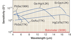
At the other end of the cost spectrum, high-end applications such as aerial imaging or long-range surveillance require higher frame rates and greater resolution. The most straightforward way to improve performance is to increase the sensitivity and the size of the detector array (see Fig. 3). Large-format MCT cameras can operate at 100 frames/s at full image size with digitized output of 14 bits of dynamic range.
A different approach that can lead to the same result is to correlate images captured at different wavelengths. It is common in infrared imaging that the object of interest, while clearly distinguishable in the visible, has the same "infrared color" as the background. In multispectral imaging, the target is imaged simultaneously onto two or more separate detectors with different spectral sensitivities.
It often happens that the contrast difference between a target and its background, while small, reverses sign over an IR range, say within 3 to 5 µm. A detector that integrates this entire spectrum will average out the difference. Imaging the target onto two separate detectors, inverting the second signal and summing it with the first will enhance rather than cancel the difference. It is expected that high-end systems in the future will all include some form of multispectral imaging.
Still in the lab, but . . .
As the percentage of mercury in the MCT alloy is increased, which is necessary to narrow the bandgap, its material properties degrade, and so large arrays of MCT for use at 8 to 12 µm are impractical. Two other technologies promise to compete for high-end thermal detection: antimonide-based detectors, and quantum-well IR photodetectors (QWIPs).
Detectors made of alloys of indium, gallium, and mixed with antimony can be tuned to detect, with high quantum efficiency, any of the wavelengths of interest by varying the alloy proportions. Developing a new semiconductor material is difficult, however, and it may be a while before this technology lives up to its potential. QWIP detectors, on the other hand, are already in commercial products. Based on gallium arsenide technology, QWIP detectors can be made in large-format arrays that work well for multispectral sensing. They require cryogenic cooling, however.
There is keen interest in raising the operating temperatures for photovoltaic infrared detection. One approach is to sandwich a layer of MCT between two materials with wider bandgaps. Under reverse bias, this structure sweeps out the minority carriers—the electrons—from the MCT so rapidly that they do not have time to recombine with the holes.
Since this recombination leads directly to dark current, reducing this rate effectively makes the material darker than it is in thermal equilibrium. This so-called "negative luminosity" acts to absorb the thermal photons generated internally in the material, reducing the need for cryogenics. While still in the research stage, this approach may lead to MCT arrays in mid-wavelength IR imagers that use only TEC cooling.