Perhaps the fastest changing but most challenging aspect of optoelectronics is the field of optoelectronic integrated circuits (OEICs). Engineers have long known that there are potentially great savings to be achieved by putting optical components—for example, photodetectors—onto the same chip with electronic devices such as transistors. But fabrication problems and incompatibility of materials have kept these devices from being fully realized until recently. Now, some of these OEICs are almost ready to move into the marketplace.
The appeal of integration of optical and electronic devices on a single chip is that it eliminates the headaches created by separate packaging. When the devices are physically separate, each electrical interconnection generates parasitic capacitances and inductances that slow circuit response. In addition, in fiberoptics, wavelength division multiplexing (WDM) requires that multiple sets of receivers and transmitters be linked by a single fiber. Without integration, the problem of multiple fiber alignments becomes daunting. By integrating the photodetectors, amplification circuits, and demultiplexing and fiber interconnections on a single chip, sensitive fiber connections can be done in a single step, rather than once for each receiver set.
So far, the main application of OEICs is in long-distance telecommunications, for which the highest performance is demanded. With WDM, end-to-end integration can achieve potentially large performance improvements. At the transmitter, lasers and driver electronics can be integrated with multiplexing fiber connections feeding into a single fiber. At the other end, receivers can integrate local oscillators, mixers, demultiplexers, photodetectors (either p-n junctions or avalanche photodiodes [APDs]), and spot amplifier circuits (see photo). The idea would thus be a configuration consisting of two chips and one connecting fiber. Integration, combined with erbium-doped fiber amplifiers, can potentially make the cheaper p-n detectors as efficient as the more-complex APDs.
Another possible application is in very-short-distance connectors, replacing copper wires with integrated fiberoptic circuits. Fibers have superior performance over distances greater than 10 m at bit rates beyond 1 Gbit/s. An example of such an application would be rack-to-track connections among high-speed computers or electronic signal-processing equipment. Here, however, rapid and continuous improvements in interconnections and packaging make this application area a moving target for OEICs.
Integration approaches
The basic problem to be overcome in integrating optoelectronic and electronic devices is the incompatibility of the materials involved. At the infrared wavelengths used in fiberoptic communications, silicon is transparent, so most detectors are based on III-V semiconductors such as gallium arsenide (GaAs), indium gallium arsenide (InGaAs), indium phosphide (InP), or related materials. But, of course, electronics are generally silicon-based for low cost and because of the enormous industrial base for existing silicon processing.
There are a number of incompatibilities between the two types of materials. For one thing, the lattices are mismatched so that it is difficult to grow one layer on top of another without producing massive numbers of defects. Second, photodetectors require very pure layers of absorptive material, while a typical transistor, such as field effect types (metal-semiconductor field-effect transistors [MESFETs], for example) requires narrow layers doped at hundreds of times higher levels as could be allowed in photodetector absorption layers. In addition, photodetectors normally are grown on negatively doped substrate and have metal contacts on both top and bottom, while FETs are grown on semi-insulating substrate with electrodes only on the top.
The trick is to develop a technique that can process both types of materials together or to somehow avoid the problem altogether. There are a number of approaches to solving this problem.
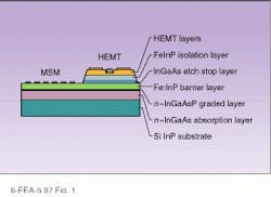
Perhaps the simplest approach is to just use compatible materials. After all, GaAs electronics are well developed although they tend to be more expensive than their silicon counterparts. For example, metal-semiconductor-metal (MSM) photodiodes and GaAs MESFETs can be grown together on GaAs substrates with the electrodes of the photodiodes interdigitated with the absorbing areas. Such a design has the disadvantages that the absorption layer is partially shadowed by the transistors and that using GaAs technology increases costs. However, the MSM structure has very low capacitance, and the overall structure is quite simple (see Fig. 1). This is one of the designs that has been commercialized.A bit more complicated approach is to tack the layers for one device on top of the layers for the other, using compatible compounds for both devices. The top layer is removed where appropriate during processing. One intrinsic problem with this approach is capacity coupling between doped layers of the two devices.
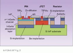
For example, a junction FET transistor’s layers can be grown over layers for a PIN photodetector (see Fig. 2). Here two problems have to be overcome: the InGaAs absorption layer is too highly doped to act as an insulator below the transistor channel, and there is a highly conducting n-doped layer a few microns below that. In processing, these problems can be overcome by selective ion implantation to change the characteristics of the wafer under the two devices.Because the photodetectors tend to be much "taller" structures than the transistors, several microns of material have to be etched away to get to the transistor layer. This precludes using very narrow lines, because the etched trenches cannot be made steep enough. The common alternative is to cut away part of the wafer and recess the photodiode so that the transistor layers are near the top. This approach requires careful optimization of the process to avoid anomalous, unwanted growth at the edges of the crest.
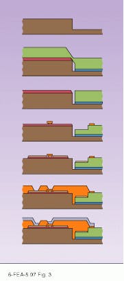
To get the same PIN with FET in this approach, a recess 3.5 µm deep is etched into InP substrate. A complex cycle of growth and etching can then result in the two devices being nearly side by side, with their top surfaces level, allowing the transistor to have finer lines (see Fig. 3).Matching incompatibles
These approaches all assume that the materials used are compatible—that is, they preclude the use of low-cost silicon-based circuits. To integrate incompatible materials requires other techniques. One of the easiest and oldest is flip-chip bonding. The idea in this well-tested and long-used technology is to bond two devices back-to-back on the same chip using indium or solder bonds. Parasites are avoided, and the assembly is rugged—two main advantages of integration—but little modification to either device is needed. A second method of avoiding the problems of lattice incompatibility is to grow each device on its own substrate, then remove one of the devices from its substrate and transfer it to the other. This technique is known as epitaxial liftoff or film grafting.
A relatively new and promising approach to integration is wafer fusion, which also allows incompatible materials to be used together. In this technique, briefly referenced in Back to Basics last month (see Laser Focus World, May 1997, p. 203), layers of one material, say InGaAs, are grown on InP substrate. At the same time a silicon transistor is grown on a silicon substrate, as in epitaxial liftoff. The top layer of one device is then fused to the top layer of the other device by placing the two wafers in direct connect under pressure at high temperature (around 65C) in a hydrogen atmosphere. The substrate of the top wafer is then selectively etched away, leaving two intimately bonded devices.
More integration
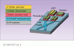
While much attention has been focused on just getting a photodiode and a transistor together on a chip, researchers are also working on more ambitious schemes. For example, for coherent receivers, waveguides, optical couplers, and switches can be incorporated on a chip by cutting groves into the substrate (see Fig. 4). A further step is to add a laser diode and its associated control and modulation circuits to achieve a fully integrated optical repeater. Such advanced OEICs have been fabricated in the laboratory but are still far from commercialization.For lower levels of integration, however, commercialization finally seems imminent. Just at this crucial time, unfortunately, research funding has been radically decreasing. This has already affected the rate of progress in integration and may threaten the achievement of fully integrated circuits, which seem well within reach technically.
Eric J. Lerner | Contributing Editor, Laser Focus World
Eric J. Lerner is a contributing editor for Laser Focus World.


