Imaging options expand with CMOS technology
Imaging options expand with CMOS technology
Jeffrey Zarnowski and Matt Pace
To build the best imaging system for an application, designers must decide between traditional imagers, those with partially integrated electronics, and those with totally integrated on-chip electronics.
In the early 1970s, with metal-oxide semiconductor fabrication becoming commonplace, the three traditional solid-state imager technologies--charge-coupled-device (CCD), charge-injection-device (CID), and photodiode array (PDA)--became viable alternatives to imaging tubes. Standard complementary metal-oxide semiconductor (CMOS) processing matured by the mid-1980s, and by the early 1990s, designs calling for a million or more transistors were commonplace for digital systems. Devices of this magnitude incorporated large die areas and required high yields. With standard CMOS processing techniques, it was now practical to fabricate solid-state imagers of useful size and quality.
The rise of CMOS-based imagers and the application of the technology to existing detectors have presented applications engineers and scientists with a broader range of imaging options (see Laser Focus World, April 1997, p. 73). Although these options add a level of design freedom, they also add an extra layer of confusion to the process of determining the best possible imager for a given set of price and performance requirements. These CMOS imagers can be categorized either as traditional devices augmented by CMOS processing or as "true" CMOS imagers with passive- or active-pixel sensors. Both categories offer the user new and improved capability but have limitations that the designer must understand when choosing between them.
Integration with traditional imagers
The move to CMOS processing brings electronics on-chip for improved functionality and simplified system interfacing that should lower system costs. Standard, functional off-the-shelf parts available to the board designer are now available to the imager designer. This approach shifts much of the burden of process development, improvement, and characterization to the wafer fabricator.
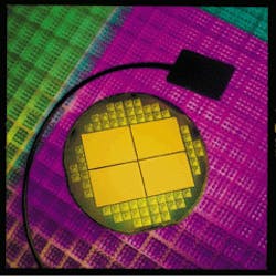
By shifting imager designs to CMOS processing, designers can implement many camera functions on-chip. All three of the traditional solid-state imager technologies--CCD, CID, and PDA--have been adapted to allow integration of CMOS electronics, which can include clock drivers, self-scanning, self-biasing, synchronization, clamp, gamma, color correction, and auto gain control (see photo above). Many of the functions that were previously performed by a frame grabber or that required external control can now be implemented on-chip as well.
The argument that the increased complexity and die size will limit device yield and actually increase cost over conventional imagers is not true. For example, the use of CMOS technology increases the die size of a 0.33-in. black and white "camera on a chip" by only 20%, to 0.4 in., which is still smaller than a typical frame-transfer CCD of the same format.
Existing proprietary fabrication flows to produce imagers have been expanded to include the necessary CMOS process steps. The down side to this integration is that it actually increases the number of masks and process steps involved and, therefore, system cost. The approach manufacturers take on adapting CMOS processing steps will determine whether they are able to shop for competitive pricing and shift their process development, improvements, and characterization to the wafer foundry.
Conventional imager technology augmented by CMOS electronics offers increased operating speed at reduced power. Designs can also be simpler, and thus more compact, than conventional systems. To maintain the expected dynamic range, however, the traditional 10-V operating bias must still be maintained. The greater the biasing the greater the full well of the pixel, so high operating voltages in turn require designs to be implemented using feature sizes greater than 2 µm. Designs based on 5-V operating biases can be implemented, but this cuts the dynamic range at least in half. Finally, simply porting a traditional imager technology to CMOS fundamentally won`t increase or reduce noise associated with the pixel structure.
True CMOS imagers
Standard CMOS processes rather than modified proprietary processes are being used to construct true CMOS imagers, including photogate and photodiode devices. A photogate device is similar to a CID or CCD in that a pixel is constructed of a MOS capacitor. Photodiode pixels are easily constructed in CMOS process, because pixels are defined by an exposed silicon junction.
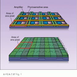
True CMOS imagers incorporate an amplifier at or near the pixel site, so only one row and column are necessary to address a pixel (see Fig. 1). Power consumption is thus very low in comparison with CCDs, in which the entire contents of the array must be transferred. In comparison to traditional imagers, CMOS devices suffer from increased dark current, caused by the highly doped silicon required by submicron processes; higher dark current leads to increased image noise. The imagers also suffer from slightly reduced sensitivity at longer wavelengths, caused by the lower resistivity of the wafer material.
CMOS imagers can be further classified as active- or passive-pixel sensors. An active-pixel sensor (APS) consists of randomly addressable pixels with an amplifier at each pixel site. This amplifier placement results in lower noise levels than with CCDs, in which the charge is coupled to the amplifier, or with PDA or CID structures, in which the collected signal at the pixel site is degraded by long bus runs before reaching the amplifier, often located off-chip.
Currently available APS structures offer video-rate operation with noise levels of less than 100 electrons. As always, however, there are trade-offs. The devices suffer from relatively slow readout, reduced sensitivity, and increased fixed pattern noise (FPN). Each pixel must have addressing and biasing buses; in conjunction with the amplifier, these buses block a sizable portion of the photosensitive area of the pixel, reducing device sensitivity. The small amplifiers, a fraction of a pixel in size, must drive the signal down long polysilicon and metal buses with time constants on the order of microseconds, reducing readout rate. The actual addressing process causes instability on the substrate, which affects the image quality. As array size increases, operating speed drops further.
In comparison to a CCD, the complex pixel structure of an APS device offers more opportunity for subtle mask deviations and processing variations to affect pixel sensitivity and amplifier characteristics. Correction circuitry for FPN correction must be added to eliminate deleterious effects.
Advocates of CCDs assert that APS sensors will be unable to achieve the pixel count, array size, or pixel size of CCD imagers, but this is incorrect. Traditional CCD imagers, with their high biasing requirements, are forced to use feature sizes of 2 µm or larger. True CMOS imagers can be fabricated using deep submicron processes to produce features as small as 0.35 µm, fitting up to eight transistors into the space required for a single transistor with 2-µm features. As development progresses, high-resolution lithography will allow APS sensors to achieve equal or greater sensitivity than interline transfer CCDs.
Passive-pixel sensors
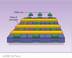
Passive CMOS sensors use standard CMOS processes with on-chip video amplification. To overcome the lower biasing requirements and improve noise characteristics of passive pixels, photogates or photodiodes feature an amplifier at the end of each row or column, along with FPN correction circuitry (see Fig. 2). With more exposed silicon to capture photons and a larger full well than a comparable APS, passive-pixel devices have greater responsivity than active ones.
The simplicity of the array structure reduces the chances of pixel defects, increasing yield and reducing cost in comparison to a CCD or APS device, in which a pixel defect has a greater chance of triggering a row or column defect. The performance trade-off in passive pixel sensors is noise. Caused by the placement of amplifiers at the periphery of the array, noise typically ranges from 100 to 2000 electrons.
To illustrate the versatility of CMOS imaging technology, consider an imaging system on a chip designed by engineers at Integrated Electronic Technologies (IET; Cicero, NY). The imaging area consists of a 600 ¥ 800 array of 39-µm pixels. Featuring on-chip self-scanning and self-biasing electronics, the device, once initiated, reads out one frame of video and provides required synchronization information as well. This device is produced at a fraction of the piece cost of a CCD.
Performance trade-offs
Often we at IET are asked, "What is the performance of your typical imager?" Unfortunately there is no "typical imager"--the solutions designed to meet the needs of the various applications are as varied as the applications themselves. Designers must recognize that a CMOS imager is not simply an imager, but an imaging system. It is necessary to compare specifications carefully. The CMOS imager, often containing scanning, biasing synchronization circuitry, and video buffering, will also include system-related noise. For the majority of applications, the overall signal-to-noise ratio (SNR) is most important. System designers often believe that the lower the imager noise, the better the performance. In fact, optimal SNR in a system that satisfies applications-specific secondary and tertiary requirements is most important. Too often, lack of understanding may drive the designer to select a more familiar, but less cost-effective solution.
Just as application needs vary, so will imager-based camera systems. No CMOS imager will satisfy every application, and there are finite limits to the practical uses of the technology. For example, the devices will not in the foreseeable future be available to the ultralow-noise scientific market--that niche will remain filled by the CCD or CCD/CMOS hybrid. Although more radiation-tolerant than CCDs, CMOS imagers will never be as robust as the p-channel MOS CID, which will continue to control that market sector. A photodiode array can be read in a nonintegration mode, so applications requiring this performance will remain outside the province of CMOS imagers.
For the vast majority of the imaging market, however, these less-common requirements are overshadowed by the demand for ultimate value. The piece-cost-versus-performance winner will in every instance be the CMOS imager. The combination of standard CMOS fabrication and on-chip electronics to lower external system costs yields the most economical solution. As CMOS imagers become more commonplace and functionality increases, the cost of imaging for a given application will continue to drop.
Increased functionality offered by CMOS imagers now includes partial or complete integration of electronics, random access, variable integration time, video processing, background subtraction, and digitization. Future systems will feature smart sensor systems, video compression to minimize bandwidth, smart pixels, and application-specific integrated circuit subcells.
Decision-making imagers
The designers at IET are currently developing a smart-pixel device that will incorporate decision-making ability into a pixel. Decision-making video processing currently performed by software and/or hardware will be moved to the imager, increasing throughput. To add perspective to the potential of the CMOS imager, one has only to understand that any electronics, any function, any standard part that can be created with CMOS processing can be added seamlessly to a CMOS imager. Ultimately, the CMOS imager will become a standard cell available in an ASIC library for the user to configure as needed. There are no technical barriers to the eventual realization of a full-resolution camera on a chip for less than $10.
Custom imagers can be produced affordably. CMOS processing techniques are driving down the nonrecurring engineering costs of custom imagers. Custom application-specific imaging systems can be designed, prototyped, and made production ready for as little as $250,000. System designers armed with knowledge of CMOS processing techniques and advantages can more easily determine the most-appropriate technology for a given application, whether it is an off-the-shelf or a custom system. o
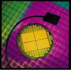
By using CMOS technology to implement charge-injection device architecture, designers were able to fit both detector and scanner electronics on the same wafer.
FIGURE 1. Traditional three-phase, full-frame CCD (top), with its attendant fixed readout scheme shifts charge along the column into the serial row register where the row register shifts all the pixel data out to an amplifier. CMOS-based active-pixel sensor (bottom) features an amplifier at each pixel to reduce noise. The amplifiers and buses block a portion of the photosensitive area of each pixel, reducing device sensitivity.
FIGURE 2. Passive-pixel CMOS imager features randomly addressable pixels with amplifiers at the end of the columns. Instead of the photon-generated charge being amplified directly, as with CCDs or APSs, the signal is read at a distance and can be degraded by the bus resistance and capacitance.


