Designers still choose mercury cadmium telluride
Despite attempts to replace it with alternatives, mercury cadmium telluride remains the most important material for infrared photodetectors.
Jozef Piotrowski and Fred Perry
During the past three decades mercury cadmium telluride (Hg1-xCdxTe) has been the most important semiconductor for mid- and long-wavelength (l = 3-30 µm) infrared photodetectors. After silicon and gallium arsenide, it is one of the most important semiconductors for any purpose. The spectral range of 3-30 µm is important for remote temperature sensing and thermal imaging. No single known material surpasses Hg1-xCdxTe in fundamental performance and flexibility. Moreover, Hg1-xCdxTe exhibits nearly constant lattice parameters, which is of extreme importance for fabrication of new devices based on complex heterostructures. Initially, the success of Hg1-xCdxTe stemmed from the fact that the compound with x = 0.2 was the only well-behaved intrinsic semiconductor with ڤ.1 eV band ga¥for 8-14 µm photodetectors.
There have been numerous attempts to replace Hg1-xCdxTe with alternative materials such as similar alloys of zinc (Zn), manganese (Mn), and tin (Sb). At present, several other variable-ga¥alloy systems are known including the closely related alloys Hg1-xZnxTe, Hg1-xMnxTe, lead tin tellurides and selenides, InAsSb, III-V compounds with thallium, and bismuth free-carrier detectors and low dimensional solids.1-3
The motivations behind the attempts to replace Hg1-xCdxTe are technological. One problem is a weak HgTe bond, which results in bulk and surface and interface instabilities. Uniformity and yield are also issues. But none of the new materials offers fundamental advantages over Hg1-xCdxTe. The most important parameter of infrared detectors is detectivity--the normalized signal-to-noise ratio. The detectivity of any type of infrared photodetector is proportional to (a/G)1/2, where a is the absorption coefficient and G is the thermal generation rate. While this figure of merit of various narrow-ga¥semiconductors seems to be very close to that of Hg1-xCdxTe, the free carrier detectors and GaAs/AlGaAs superlattice devices have several orders of magnitude smaller values of a/G. Hg1-xCdxTe also exhibits extreme flexibility. It can be tailored for optimized detection at any region of the IR spectrum.
The present development of infrared photodetectors has been dominated by complex band-ga¥heterostructures. Among various variable-band-ga¥semiconductor alloys, Hg1-xCdxTe is the only material covering the entire IR spectral range having nearly the same lattice parameters. The difference between CdTe (Eg = 1.5eV) and 0.1 Hg0.8Cd0.2Te is ڤ.2%. Replacing a small fraction of Cd with Zn or Te with selenide (Se) can compensate for the residual lattice mismatch. The independence of lattice parameters on composition is a major advantage of Hg1-xCdxTe over other materials.
Heterostructures do not offer any inherent advantages over homostructures for conventional equilibrium-mode devices. The fundamental limits to performance of infrared detectors are imposed by unavoidable optical and thermal carrier generation in the narrow-ga¥base region of a photodetector. Nevertheless, heterojunctions are helpful in achieving high performance in practice. For example, the narrow-ga¥Hg1-xCdxTe that absorbs infrared radiation can be buried or encapsulated in wider-ga¥Hg1-xCdxTe, preventing instabilities due to the weak HgTe bonds. In addition, heterostructures can be used for nonequilibrium devices with potential performance much higher than conventional structures.4
Epitaxial growth techniques
Epitaxy is the preferred technique to obtain device-quality HgCdTe epilayers for infrared devices. In comparison to bulk growth techniques, epitaxial techniques offer large areas and sophisticated structures with abrupt and complex composition and doping profiles that can be configured to improve photo- detector performance. Epitaxial growth can be performed at low temperatures, which makes it possible to reduce native defect density. Due to the low mercury pressures there is no need for thick-walled ampoules, and growth can be carried out in reusable production-type growth systems. As-grown epilayers can be low-temperature-annealed in situ. Epilayers can be used for IR devices without troublesome and time-consuming thinning.
Among the various epitaxial techniques, liquid-phase epitaxy (LPE) is the most mature method, enabling growth of device-quality homogeneous layers and multilayered structures. The LPE growth process must be performed at relatively high temperatures with adherent interdiffusion and resulting graded interfaces. Recent efforts center mostly on low-growth-temperature techniques--MOCVD and MBE. Metal organic chemical-vapor deposition (MOCVD) is a nonequilibrium method that appears to be most promising for future large-scale and low-cost production of epilayers. The advantages of this method are reduced growth temperature and the ability to modify conditions during growth to obtain desired band-ga¥and doping profiles.
Intensive studies are currently under way on molecular beam epitaxy (MBE). This technique offers unique capabilities in material and device engineering including the lowest growth temperature, superlattice growth and potential for very sophisticated composition and doping profiles. Computerized control of MBE systems is easy. The main drawback of both MOCVD and MBE is the high cost of equipment and maintenance.
Since 1980 at VIGO System in Warsaw we have used isothermal vapor-phase epitaxy (ISOVPE) for manufacturing of a variety of infrared photodetectors operated at and near room temperature, including photoconductors and photoelectromagnetic and photovoltaic devices. Unconventional three-dimensional heterostructure devices have been developed to optimize operation at near room temperatures. Initially invented in France, ISOVPE is one of the oldest epitaxial techniques applied to grow HgCdTe on CdTe substrates.5 It is a relatively simple, quasi-equilibrium growth technique in which HgTe is transported at a relatively high temperature (400C-600C) from the source (HgTe or Hg1-xCdxTe) to the substrate by evaporation/condensation mechanisms. While very good lateral uniformity of composition can easily be obtained, an inherent property of the method is in depth grading, because some interdiffusion of deposited and substrate materials is involved in layer formation. Extremely uniform epilayers can be obtained. This process requires substrates matched structurally, chemically, and mechanically to Hg1-xCdxTe to prevent defect formation and uncontrolled doping.
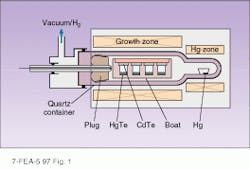
We have developed a production-type reusable atmospheric pressure system for ISOVPE that allows a large area of multiple layers to be grown in one growth run (see Fig. 1).6 Mercury loss problems are practically eliminated by the use of a quart¥assembly consisting of a container closed by a conical quart¥plug. Very low mercury loss was found--a few milligrams per growth run. In-depth band-ga¥profiles have been shaped in controlled ways by variations of growth conditions and subsequent post-growth annealing. The necessary growth conditions can be theoretically predicted using computer simulation of ISOVPE based on our generalized model of the process.7 Layers from <1 µm to >1 mm thick and surface compositions where 0As-grown epilayers exhibit a significant grading. If the growth stage is followed by heat treatment at temperatures lower than the deposition temperatures (300C-400C) with deposition suppressed by increased mercury vapor pressure, nearly uniform composition in most of the layer (ڦ/3 of total thickness) can be obtained. A significant grading in the bottom portion of the layer occurs. In addition, post-growth thermal processing (that is, negative epitaxy) has been used to widen the band ga¥of the region near the surface. In contrast to LPE, MOCVD, and MBE, smooth surface morphology can be obtained by ISOVPE independent of substrate orientation for growth temperatures greater than 500C. This makes it possible to grow epilayers on unoriented substrates, an important advantage of this growth technique.
Regarding electrical properties, as-grown layers always exhibit p-type conductivity due to doping with native acceptors, which are metal vacancies. To reduce the number of vacancies, the growth process is completed with programmed cooling of the growth and mercury zones to room temperature. Low electron concentration (1015 cm-3) is typically obtained. These carrier concentrations probably result from impurities in the substrates, source materials, gases, or contaminants on the substrate surface.
Initially, doping levels were controlled by heat treatment in mercury vapor. The resulting concentration was determined by the difference between concentrations of native acceptors and residual donor impurities. At present, the required doping is achieved with foreign impurities (In, Au, and As). The basic material for most near-room- temperature devices is a lightly doped p-type layer in which As and Au are introduced into epilayers in situ during growth. This approach integrates growth and device fabrication. Some devices require additional ex situ doping achieved by diffusion of dopants and/or ion milling.
Three-dimensional band-ga¥profiling is necessary to optimize photodetectors.8 We have developed several methods to modify in-depth lateral band-ga¥profiles including removal of some portions of the epilayer grown by ISOVPE, growth on patterned substrates, regrowth, selective epitaxy, and negative epitaxy. These methods require advanced wet and dry techniques combined with advanced photolithography.
Infrared devices
Infrared photodetectors are based on the principle of optically generated carriers detected as a change in voltage or current across the element. Recent advances in heterostructure devices such as development of heterojunction photoconductors, double-layer heterostructure photodiodes, and nonequilibrium modes of operation make this distinction no longer so clear, however.
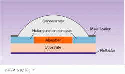
In an optimized photodetector, a lightly doped narrow-ga¥semiconductor region acts as an absorber of IR radiation (see Fig. 2). Its band gap, doping, and geometry should be selected for the highest ratio of optical-to-thermal generation rates. The electric contacts to the narrow-ga¥region that sense optically generated charge carriers should not contribute to the dark current of the device. The narrow-ga¥region must be passivated: the surfaces of the absorber regions must be insulated from the ambient by a material region that does not contribute to the generation of carriers. In addition, the carriers that are optically generated in the narrow-ga¥absorbing region must be kept away from surfaces where recombination can reduce the quantum efficiency. For the best sensitivity, the front face of an optimized photodetector should perfectly transmit IR radiation. Finally, a concentrator of IR radiation such as an immersion lens should be included where possible, as should a reflective backside mirror region to reflect the IR radiation and maximize absorption.
In practice, such a device can be obtained using three-dimensional ga¥and doping engineering, with the narrow-ga¥absorber buried in a wide-ga¥semiconductor. The undoped wide-ga¥material can be used as a window, and/or a concentrator of incoming radiation. Doped n- and p-type semiconductors are used for contacts. The device must be also supplied with contact metallization and electrical leads. Thermal generation in the contact regions is virtually eliminated by making them wide gap.
Photoconductors were the first long-wavelength Hg1-xCdxTe infrared devices for operation near room temperature. Three-dimensional band-ga¥profiles with absorber regions covered with wide-ga¥material and heavily doped contact regions are a standard design.8,9 Strong electric fields are required to achieve the fundamental limits of performance when the devices are operating at or near room temperature. This results in high flicker (or 1/f) noise, which can dominate even at frequencies greater than 1 MHz. Bias power dissipation prevents use of photoconductors for large-area single-element devices or two-dimensional arrays. These limitations are especially severe for long-wavelength devices operating at room temperature or with Peltier coolers.
Photovoltaic detectors have important advantages for operation near room temperature.8,10 No bias is necessary, which prevents the occurrence of flicker noise and ohmic heating. The short diffusion length and weak absorption of radiation in narrow-ga¥semiconductors make it difficult to obtain useful performance of long-wavelength photovoltaic devices operating near room temperature using conventional device designs. Even more serious problems are caused by extremely low junction resistance and low voltage responsivity. For example, resistance and voltage responsivity of an uncooled 10.6-µm device with an active area of 1 ¥ 1 mm are as low as 䉲-3 and ڦ&10-3 V/W, respectively.
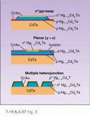
Poor quantum efficiency and low dynamic resistance found in conventional long-wavelength infrared photovoltaic detectors when operated near room temperature can be overcome with development of multiple heterojunction photovoltaic devices in which short elements are connected in series.8,10,11 Theoretically, this makes it possible to obtain complete absorption of incident radiation, high collection efficiency, and high resistance and voltage responsivity (see Fig. 3).
Imaging and nonimaging applications
The most important of the present generation of thermal imagers are based on linear Hg1-xCdxTe photoconductive arrays operated at or near liquid-nitrogen temperature. Increased sensitivity can be achieved by using two-dimensional multiplexed arrays of photovoltaic detectors operated in either scanning or staring mode. Staring Hg1-xCdxTe focal-plane-arrays are now available in various formats u¥to 1024 ¥ 1024.12 Thermal imagers with large staring arrays do not require any moving parts, which reduces system size and complexity. Thermal resolution of less than 3 mK has been already reported for imagers operated at 95 K in the 3.4-4.8-µm band.
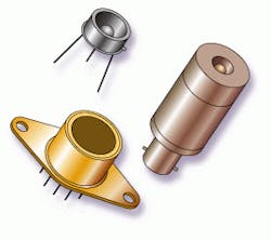
Most of the devices currently manufactured by Vigo System are used for applications other than thermal imaging. Examples are fast pyrometers, analytical instruments, laser radiation monitors, intruder alarms, homing heads, guidance of intelligent munitions, and laser threat-warning receivers. While single-element or small arrays are typically used in these applications, some of them are quite demanding regarding performance, speed of response, and temperature of operation (see figure on p. 135). Monolithic optical immersion is widely used to improve performance of the devices.
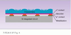
Despite a great R&D effort, Hg1-xCdxTe photodetectors remain expensive, primarily because of the low yield of good devices and the cost of substrates. Future generations of infrared systems will require high-performance, cost-effective staring arrays that operate near room temperature. In this arena, Hg1-xCdxTe will compete with thermal detectors, Schottky barrier devices, quantum-well devices, and possibly new variable-ga¥A3B5 alloys. Several conditions must be met to preserve the leading role of Hg1-xCdxTe. First, cost-effective device-quality Hg1-xCdxTe growth on silicon, GaAs and other readily available and inexpensive substrates should be developed. Several laboratories have already begun fabrication of Hg1-xCdxTe on silicon substrates. Such integrated fabrication may result in devices for future-generation thermal imagers (see Fig. 4).
Other fabrication challenges include the growth of heterostructures with three-dimensional ga¥and doping profiles, integration of crystal growth with array processing and preparation of optical concentrators, and multiplexer development to take full advantage of the fundamental advantages of the material. Also, the low-temperature epitaxial techniques of MBE and MOCVD must meet the requirements for fabrication of future generations of infrared photodetectors. Overcoming these challenges will ensure that Hg1-xCdxTe remains the material of choice for infrared sensing devices. o
REFERENCES
1. A. Rogalski, New Ternary Alloy Systems for Infrared Detectors, SPIE Optical Engineering Press, Bellingham, WA (1994).
2. A. Rogalski, Infrared Photon Detectors, SPIE Optical Engineering Press, Bellingham, WA (1995).
3. Haime Asahi, Compound Semiconductor 2, 34 (1997).
4. C. T. Elliott and N. T. Gordon, "Infrared Detectors," in Handbook on Semiconductors, Vol. 4, p. 841, C. Hilsum, ed., North-Holland, Amsterdam, Netherlands (1993).
5. G. Cohen-Solal et al., Acad. Sci. Paris 261, 931 (1965).
6. J. Piotrowski et al., Thin Solid Films 161, 157 (1988).
7. Z. Djuric and J. Piotrowski, Appl. Phys. Lett 51, 1699 (1987).
8. J. Piotrowski and M. Razeghi, Proc. SPIE 2397, 180 (1995).
9. Vigo System (Warsaw, Poland), Data sheets (1997).
10. J. Piotrowski and W. Gawron, Infr. Phys. and Technol. 38, 63 (1996).
11. K. Adamiec et al., "Isothermal vapor phase epitaxy as a versatile technology for infrared photodetectors," Proc. SPIE 2999 (1997, in press).
12. L. J. Kozlowski, Proc. SPIE 3179, 200 (1997).
Mercury cadmium telluride can operate as a photodetector in various packages. Examples of optically immersed MWIR and LWIR Hg1-xCdxTe photodetectors include high-frequency (>20 MHz) ambient-temperature device (right); low-frequency (<20 MHz) ambient-temperature device (top); and Peltier-cooled detector.
FIGURE 1. Isothermal vapor phase growth reactor allows the growth of HgCdTe on CdTe substrates under atmospheric pressure.
FIGURE 2. Three-dimensional heterostructure photodetector contains HgCdTe absorber region in the center, surrounded by heterojunction contacts. Concentrator focuses radiation on absorber region while reflector back surface re-radiates radiation for maximum efficiency.
FIGURE 3. Single heterojunction photovoltaic devices can be fabricated with mesa structures (top) or in planar design in which y>x (middle); multiple heterojunction structure can be used to form array detectors (bottom).
FIGURE 4. In future infrared imaging sensors, a two-dimensional array of infrared photovoltaic detectors could be integrated with Fresnel lenses and silicon integrated-circuit image processor.
JÓzef Piotrowski is director of development at VIGO System, Hery 23, 01-497 Warsaw, Poland, and Fred Perry is president, Boston Electronics Corp., 72 Kent St., Brookline, MA 02146.
