Circuit integration pushes image sensor performance
Circuit integration pushes image sensor performance
High-performance CMOS sensors are challenging CCD arrays at the pixel level in future digital imaging applications.
Woodward Yang
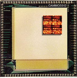
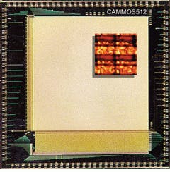
Prototype digital CMOS sensor developed at Hyundai Electronics has
512 x 512 active pixels, high-performance CMOS photosites, and integrated analog-to-digital converter arrays and clocking circuitry. Inset shows active-pixel CMOS array.
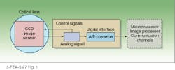
FIGURE 1. In advanced digital electronic imaging applications, the analog signal from CCD image sensor is directly digitized (A/D converter) and interfaced to microprocessors and digital
communication channels.
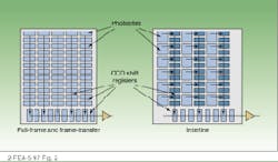
FIGURE 2. Full-frame and frame-transfer imager architecture (left) is simple and relatively compact.
Interline structure (right) is more complex but offers improved color sensitivity and reduced image smearing from having individual light-shielded shift registers.
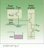
FIGURE 3. When a charge sensed by a CCD in the well is transferred into the floating p-n junction above it, the buffer amplifier at right outputs this signal as a change in voltage.
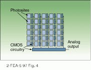
FIGURE 4. Analog output signals from any CMOS image-sensor pixel can be randomly accessed through wires and multiplexing
circuitry. Integrated MOS transistors allow
multiplexing and manipulating the analog
signal from each photosite.
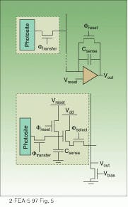
FIGURE 5. Passive CMOS pixels can be made quite small while having a large photosite, but sensitivity at low signal levels may be compromised by large parasitic capacitances in the multiplexing circuitry and by susceptibility to noise (top). An active CMOS pixel includes multiplexing circuitry and MOS transistors (bottom). Together these form a buffer amplifier with a sensitive floating input capacitance.
