High-speed CCD camera retains resolution
Integrated design produces large-area video-rate CCD camera with a readout speed of 30 million pixels per second.
George Williams, Serge Ioffa, and Jim Janesick
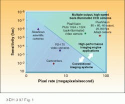
Electronic imaging has always involved a compromise between speed and other performance characteristics. While charge-coupled-device (CCD) detectors have provided the sensitivity, dynamic range, and linear response necessary for a variety of imaging applications, readout speeds have lagged, imposing performance limitations on large-array cameras. Achieving video-rate operation (30 full frames/s) with a 1024 ¥ 1024 detector array, for example, requires a readout rate of 30 megapixels per second. Until recently, output speeds for 12- and 16-bit cameras remained in the 2 to 5 megapixels/s range (see Fig. 1).
A concerted approach that simultaneously optimizes all aspects of the CCD imaging system, including control and readout electronics, is needed to increase readout rate. PixelVision Inc. (Beaverton, OR), a camera manufacturer, in collaboration with CCD fabricator Scientific Imaging Technologies Inc. (SITe, Beaverton, OR), has developed a series of integrated imaging engines capable of high-resolution image capture at speeds u¥to 60 megapixels/s. By producing an integrated package, which frees the system builder from mastering the intricacies of CCD technology, our design team has made this technology accessible to a wide range end users, while decreasing product development costs and time to market.
The speed of a CCD camera can be limited by detector design, fabrication, and clocking circuitry, by data readout, digitization, and transfer to storage, and by real-time image processing and analysis. Successful design of a high-speed system thus requires an integrated system approach involving both the CCD designer and the camera designer. For example, high pixel rates require clocking signals (to drive the CCD) at rates approaching the radio frequency (RF) regime. To achieve compatibility and minimize any clock signal distortion, the detector and associated electronics must be designed in concert. On the data side, high-speed signal amplification and digitization present similar issues of compatibility and component proximity. In addition to high performance, the integrated approach ensures simplicity of operation and integration for the OEM or end user.
Built for speed
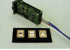
The PixelVision/SITe collaboration resulted in the Pluto series of imaging engines, based on a large-area-array design originally developed by Janesick at the Jet Propulsion Laboratory (Pasadena, CA) for a NASA mission to Pluto (see photo above). The overall goal of the design team was to achieve a video-rate, noise equivalent signal (NES) of 5 to 10 photons/pixel, while retaining high detector resolution. A number of techniques and design approaches were incorporated to achieve these apparently conflicting goals.
The fastest CCD architectures are interline arrays and frame-transfer devices. The interline array approach, commonly used in video cameras, involves masking alternate rows of pixels and represents an unacceptable loss of sensitivity for most applications. In a frame-transfer device, the pixel data are rapidly shifted into one or more "blind" or inactive areas of the CCD before being sequentially read out in the normal manner. This technique, adopted for Pluto, offers high-speed operation while retaining sensitivity.
Pixel size is also critical when designing for speed. Smaller pixels can be read out faster; however, smaller pixels also limit sensitivity and dynamic range. Taking all of this into account, we chose a 12-µm pixel size as the Pluto standard, with a 9-µm version as an option.
To enhance detector sensitivity, we used backthinning, pioneered by SITe personnel. This technique boosts the quantum efficiency (QE) sensitivity of a CCD by using the back side of the array for photon detection, eliminating light attenuation by polysilicon gate structures on the front (see Laser Focus World, Sept. 1995, p. 129). Our backthinned CCD reached QE values in excess of 0.9.
To lower amplifier noise and reduce image-transfer time, we included multiple output nodes in the design. Our goal for Pluto was a video-rate read noise of less than five electrons, a level of performance previously available only in slow-scan scientific cameras. Read noise is dominated by the on-chi¥amplifier(s) that feed the off-chi¥analog-to-digital converter(s). We minimized noise by designing our amplifiers with the smallest possible MOSFET (metal oxide semiconductor field-effect transistor).
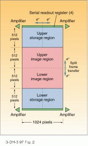
Despite the incorporation of these design elements, device performance was still limited by the fact that amplifier noise is proportional to bandwidth, which resulted in unacceptable noise for this type of amplifier at 30 mega pixels/s. To solve this problem, we went to a configuration incorporating four on-chi¥amplifiers. The active area is bidirectionally frame-transferred, and each of these half-frames is then fed into two output nodes (see Fig. 2). The output channel speeds were reduced to 10 mega pixels/s, resulting in a read noise of less than 5 e-. With a quantum efficiency of 0.9, this translates into a NES of 6 photons/pixel (better than 10-5 lux). This level of sensitivity is comparable to that of a system using an image-intensifier tube, while delivering all the usual benefits of compact, all-solid-state imaging technology. An eight-amplifier version currently under development will deliver either two times the sensitivity or the same level of sensitivity at a sustained 60 megapixels/s.
At high readout rates, the bus speed of the data storage device can become a limiting factor. Modern PCs use the high-speed peripheral component interconnect (PCI) bus. This connection has a maximum sustained transfer rate of 80 Mbit/s and can support bursts u¥to 130 Mbit/s. Used in conjunction with newly emerging serial data transfer standards, the PCI bus yields highly reliable data transfer and storage.
Clocking and fabrication
The final element in achieving high readout rates is fast charge transfer between CCD pixels. At high speeds, we have found that three-phase clocking yields optimum charge-transfer fidelity. However, this approach presents the twin challenges of fabricating small gates and interconnects and generating the fast clocking signals.
In 12-µm pixels with three phases, the smallest device structures are less than 1 µm. Silicon CCD detectors are produced by step-and-repeat microlithography. Although advanced lithographic systems can achieve minimum feature sizes of 0.2 µm, this resolution/registration is usually only maintained across a region with a 20-mm diagonal (the size of the largest commonly available integrated circuits). Fabrication of the Pluto CCDs required submicron precision across the entire semiconductor wafer (several inches in diameter), pushing semiconductor processing technology close to its current limits.
The required speed of the clocking signals also requires state-of-the-art technology. A frame rate of 30 frames/s means a frame time of 33.3 ms. To avoid image smearing, the transfer time to the dark area of the CCD should be 1% of the total frame time, in this case, 333 µs. For a 1024 ¥ 1024 array, this translates into a row-shift time of 650 ns (512 row shifts into each dark area). Each of the three phases requires two clocking signals, on the order of 100 ns.
The serial shift register operates with clocking signals of less than 20 ns, approaching the RF domain. Great care must be taken to avoid shape distortion that would affect transfer fidelity. These high frequencies also require short interconnects between the driver electronics and the CCD chip, a major reason for designing the CCD and support electronics together; the integrated design also ensures that the clock waveforms are maintained as they propagate across the CCD.
The final benefit of designing the CCD and its infrastructure in concert is ease of integration. An integrated imaging engine represents an advantage to the system builder or OEM, because it frees them from mastering the ever-increasing complexity of high-speed, high-performance CCD technology.
Applications
The high-speed imaging engine can address applications that require video-rate imaging for real-time monitoring of dynamic events, for example, fluorescence imaging of dynamic events in cell biology, such as ratio imaging of calcium ion (Ca2+) waves or enhanced night vision for military and surveillance purposes. Although airborne visible night-vision systems have already come a long way from the fuzzy green images popularized by CNN during the Gulf War, they still rely on vacuum tube technology (the image intensifier) to deliver the necessary sensitivity. Such systems are very susceptible to blooming--in scenes with local high intensities, some pixels are saturated, spilling excess photoelectrons into adjacent pixels. The Pluto imager avoids this problem with on-chi¥antiblooming protection, yielding a robust night-vision system without the high-voltage power requirements of vacuum tube designs.
The imager is also well suited to applications that require high speed simply to handle a large volume of image data, such as three-dimensional (3-D) reconstruction microscopy and film digitization. Three-dimensional reconstruction microscopy is an interesting technique in which fluorescence intensity data are recorded as a time-varying function of wavelength and xy¥position. The technique has recently emerged as an alternative to confocal microscopy, offering superior spatial resolution and multiple wavelength operation while eliminating, or reducing, photodamage to live specimens.
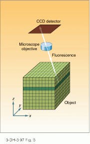
The principles of 3-D reconstruction were originally pioneered more than 20 years ago in the laboratory of David A. Agard and John W. Sedat at the University of California, San Francisco (San Francisco, CA). An array detector captures x-y image slices at a series of ¥depths (see Fig. 3). Instead of rejecting the out-of-focus fluorescence with a confocal pinhole, the technique uses Fourier deconvolution and the optical transfer function of the microscope to reassign the xy¥location of "out-of-focus" photons, producing a blur-free data cube (see Fig. 4).
Thanks to the advent of low-cost workstations, several commercial microscopes are now available, including the DeltaVision from Applied Precision Inc. (Issaquah, WA). According to Dean Waters, DeltaVision Team Leader at API, increased CCD speed and ease of integration will both be important benefits to manufacturers and end users of reconstruction microscopes. "Some of our end users record as many as 120 ¥slices in a single data set," says Waters, "and they may be imaging fluorophores at several different wavelengths. A single high-resolution data set may thus consist of more than 108 pixels of data. In dynamic (live cell) systems, this data must be recorded as quickly as possible." o
High-sensitivity Pluto imagers perform video-rate (30 frames/s) imaging with a noise equivalent signal of 6 photons/pixel (better than 10-5 lux).
FIGURE 1. Multiple-output, high-speed, back-illuminated CCD camera offers sensitivity of slow-scan scientific cameras with extremely fast readout.
FIGURE 2. Bidirectional frame transfer and multiple output nodes provide high-speed operation without compromising sensitivity.
FIGURE 3. Deconvolution microscopy allows researchers to record multidimensional fluorescence data. Images are acquired at a series of ¥depths within the object. The reconstruction algorithm "reassigns" the xy¥origin of out-of-focus light.
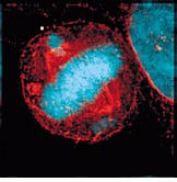
FIGURE 4. Fourier deconvolution of microscope image of mitotic spindle (red) from mouse embryonic fibroblast shows chromosomal missegregation (blue).
