Razmick Mirzoyan, Boris Dolgoshein, Arthur Barlow, and Jürgen Schilz
Typical low-light-level (LLL) applications such as astronomy, nuclear medicine, and medical imaging require measurements of the number of arriving photons over a wide range, from one up to several million photons per second, often within a narrow detection time window. Until now, the prime choice of detector has been the classical photomultiplier tube (PMT). The PMT has several disadvantages: fragile vacuum-tube construction, manual assembly, high-voltage bias requirements, magnetic-field sensitivity, and the necessity of being shielded from ambient light.
These disadvantages can be overcome by compact solid-state detectors. To date, the choice has been the avalanche photodiode (APD). The APD can operate in a classical linear mode with a relatively high noise level or in the Geiger mode as a high-speed photon counter over modest photon-count range.
More recently, the silicon photomultiplier (SiPM) increased range by using a single chip containing several hundred to thousands of micro-APD cells (microcells) coupled to a common signal output terminal. Each micro-APD is operated in the Geiger mode whereupon an arriving photon can trigger the cell, leaving the surrounding cells untriggered and ready to collect other arriving photons. The photon-counting dynamic range is comparable to the number of microcells. In the design of the SiPM, a key factor is to have the chosen number of microcells each truly independent of its neighbors—that is, having as little crosstalk as possible. Crosstalk between pixels would increase the excess-noise factor, distort linearity, limit dynamic range, and reduce time and amplitude resolutions.
A new SiPM design reduces crosstalk to a record low level because of both optical and charge isolation of the microcells. This device also has high detection efficiency and an excess noise factor very close to 1, and yet can resolve individual photons even while measuring a flux close to 100 photons/s. Such a design shows great promise as an almost ideal sensor for a variety of crucial LLL applications.
SiPM characteristics
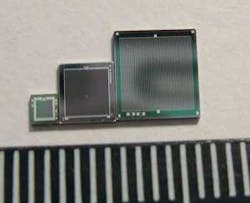
A “typical” SiPM (also known as a multipixel photon counter, Geiger-mode APD, or microchannel APD) consists of 100 to 5000 APD microcells located on a common substrate having an area of 1 to 25 mm2 with a common anode (see Fig. 1). The front surface of each microcell is connected to the power supply that creates the electrical field inside the active p-n junction. The microcells are electrically decoupled from each other through individual polysilicon resistors. The operational voltage is adjusted to a value that operates each microcell in the Geiger (self-sustained) discharge mode if it is triggered by an incoming photon. In practice, the applied voltage is 15% to 20% higher than the breakdown voltage of the APD, which is typically in the range of several tens of volts at room temperature.
The typical gain of a SiPM is 106, providing, for a single photoelectron, a signal of a few millivolts over a 50 Ω load resistor. One can consider single microcells as tiny charged capacitors (with a typical capacitance of 0.1 to 0.3 pF), which at the beginning are charged to the level of the power supply via the resistors. An incident photon initiates a Geiger avalanche process that starts to discharge the capacitor until it arrives at the breakdown voltage. Because all microcells have the identical topology, they have the same capacitance and therefore, for a given overvoltage, they provide the same fixed gain. This implies that, once fired, independent of the number of incident photons, any given microcell will produce the same charge at the anode. The charges produced from individual cells will instantly sum in the common anode. The total summed charge would be proportional to the number of fired cells. The typical dark rate of a SiPM at room temperature is 1 MHz/mm2, which is at the same level as that for a single microcell amplitude.
Efficiency
As long as the number of instantly impinging photons is less than half the total number of microcells, at first approximation a given microcell will be hit only by one photon at a time. Under this condition, the sensor output will show a linear dependence on the input light flux.
The microcell recovery time is proportional to the product of the cell capacitance and the value of the individual decoupling resistor; this product is typically in the range of 0.1 to 1 µs. While the cell is recovering (recharging), its Geiger efficiency increases toward its maximum value.
The maximum achievable photon-detection efficiency (PDE) of a SiPM is the product of the following factors: the geometrical efficiency, or the ratio of the light sensitive area of a single cell to its total area; the Geiger efficiency (this is a direct function of the applied overvoltage: 15% to 20% overvoltage can provide efficiencies in the range close to 100%); wavelength-dependent transport of impinging photons into the sensitive volume of the SiPM; and the intrinsic quantum efficiency (QE) of Si. It has been shown in Monte Carlo simulations, and verified through tests, that SiPMs can achieve a peak PDE of 50% to 60% in both the yellow-to-green and the blue-to-near-UV ranges.
Crosstalk
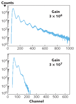
Crosstalk is an inhibiting parameter in the performance of SiPMs. The crosstalk effect is similar to afterpulsing in a photomultiplier tube, except that it exists at a much higher level and can thus inhibit achieving high sensitivity in self-trigger configurations. During the avalanche process in silicon, light is produced at a probability of around 10-5 photons/electron. Despite the very low number of generated secondary photons, they can be captured by neighboring cells, which can then be triggered to fire as well. The triggering of neighboring cells can even spread in a chain reaction. This effect violates the relationship between the incident light and produced output charge, thus creating an excess noise factor. Crosstalk can happen in two ways (see Fig. 2): by direct capture of secondary photons in the neighboring active regions (instantaneous crosstalk), and by creation of a charge photocarrier that migrates toward the active region (this process can take up to several nanoseconds).This negative effect degrades the amplitude resolution, contributing heavily to the noise figure of a SiPM (typically the noise figure is around 1.6 to 1.7). Since the crosstalk is proportional to the applied gain, one immediate remedy would be to operate the device under relatively low gains. However, this can require the use of special low-noise, wideband amplifiers with large dynamic range, thus complicating the setup.
Crosstalk reduction and resulting benefits
To diminish crosstalk, barriers on the borders of APD cells that reduce leakage currents can be produced by etching trenches. We were the first to place such trenches between microcells for optically isolating them by means of a total-internal-reflection effect; such an approach can reduce the instantaneous crosstalk.Applications
Molecular imaging is the main application driving the growth of the SiPM technology to higher volumes and to higher specification levels. One advantage of SiPMs for molecular imaging is their immunity to magnetic fields, allowing the concurrent application of magnetic resonance tomography in a single system. In addition, the reduced-crosstalk SiPM has another advantage in that the scintillator, when coupled to a SiPM, effectively acts as a mirror for silicon-generated secondary photons that boost the crosstalk.
Possible additional applications for SiPMs include dosimetry of ionizing radiation; communications detectors, including those for quantum cryptography; and safety and security systems. In research, SiPMs are applicable to a wide range of applications in astronomy and astrophysics, in biology and biochemistry, and in high-energy and particle physics; they are ideal devices to detect photons from scintillators and fibers. Large research projects, such as the development of the Cherenkov Telescope Array (a ground-based gamma-ray instrument) may call for large quantities of these detectors.
In addition to the anticipated cost advantage of SiPMs over PMTs, key advantages include two to three times higher photon-detection efficiency, better time and amplitude resolution, a compact size, and an overall reduced system complexity.
Razmick Mirzoyan is senior scientist at the Max-Planck-Institute for Physics, Munich, Germany; and Boris Dolgoshein is a professor at the Moscow Engineering and Physics Institute, Moscow, Russia. Arthur Barlow is global director of engineering, Detection Solutions, and Jürgen Schilz is product line manager, Photon Detection, at PerkinElmer, Wiesbaden, Germany; e-mail: [email protected]; www.perkinelmer.com.


