ADVANCED CAMERAS: Single-photon-counting camera operates at high frame rates
FRANCO ZAPPA, SIMONE TISA, FABRIZIO GUERRIERI, and NICK BERTONE
Single-photon avalanche diodes (SPADs) are used in applications such as LIDAR, fluorescence-correlation spectroscopy, fluorescence-lifetime imaging, particle sizing, and a host of others. Until recently, SPADs were limited to point detectors or an array with a limited number of pixels. As an example of a single-point detector, a photon-counting detector made by Micro Photon Devices (Bolzano, Italy) uses a custom silicon process to achieve high detection efficiencies, less than 10 dark counts/second, and 30 ps timing resolution. To achieve this level of performance, the SPAD fabrication process is optimized to achieve the best optical throughput, while the electronics for the quenching of the SPAD and the timing circuit are separate from the device itself.
In applications in which the highest detection efficiency, lowest dark counts, and fastest timing resolution are required, these point detectors excel. The approach of building an optically optimized SPAD and having the electronics separate can be extended to multipixel arrays, but the number of pixels to which it can be extended is limited. Having each pixel individually addressable by separate electronics has been done for an eight-element module and even for a 60-element module.1, 2 However, separating the electronics from the pixels requires a complex semicustom fabrication process to accommodate the connections; extending this approach to hundreds of pixels is not possible or feasible.
Evolution to a 32 × 32 photon-counting camera
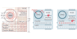
Researchers in the SPADlab at Politecnico di Milano have produced a 32 × 32 single-photon-counting array in which each pixel has all its electronics and a counter incorporated within the pixel (see Fig. 1). The pixels are 100 × 100 µm in size, resulting in a pitch (pixel-to-pixel distance) of 100 µm. The SPAD and all the electronics are fabricated using a standard high-voltage CMOS process, allowing complex electronics to be processed at the same time as the SPAD.
When the array is in use, an avalanche current builds up once a pixel detects a photon; the pixel’s variable-load quenching circuit (VLQC) senses the avalanche, quenches the current, and resets the SPAD so that it is ready to detect the next photon. After each avalanche, the quenching circuit provides an output pulse to the counter, which is a digital circuit that counts the number of detected photons and dark counts within the frame time slot selected by the user. In an operation performed at the end of each frame, the array global electronics applies a stop pulse, which stores the number of events recorded by the counter into the temporary storage register; then a start pulse resets the counter, marking the beginning of a new frame.
Array architecture
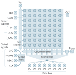
The array architecture in the 32 × 32 photon-counting camera has fully parallel operation (see Fig. 2). The beginning of each frame is marked by a stop followed by a start signal applied simultaneously to all pixels. The pixels detect and count incoming photons during each frame, while at the same time the storage register is holding data accumulated in the previous frame; therefore, data can be read out while the array captures the current frame. The maximum achievable frame rate is limited by the time necessary to read out all the data from the array. With a 100 MHz system clock, each pixel is read out in 10 ns; therefore, the maximum frame duration for a 32 × 32-pixel array is 10.25 µs, which corresponds to a continuous frame rate of about 100,000 frames/s. In addition, the on-chip global electronics provide imaging flexibility by allowing the user to arbitrarily select any desired sub-area of the array, thus increasing the overall speed. For example, selecting an area of 10 × 10 pixels results in a speed that tops 1,024,000 frames/s.The key benefit is that this 32 × 32 imager can achieve measurements of very low light intensity at very high frame rates, down to a single photon per frame. The cooled EM-CCD, the alternative technology that attains single-photon-per-frame sensitivity, can only achieve these levels at very low frame rates. However, there are some limitations to the SPAD technology that need to be understood before deciding which technology is best for a certain application.
The first issue is that each SPAD has a diameter of 20 µm and is embedded in a pixel of 100 × 100 µm. This results in a fill factor of only 3%; for this approach to be considered for imaging applications, the fill factor will need to be increased. The SPADlab group is exploring the incorporation of a microlens array that may allow the array to achieve a fill factor of 90%.
The second issue is that at low frame rates a SPAD array is not as sensitive as an EM-CCD because of a basic difference between the way these two detectors operate. In the EM-CCD all the electrons generated in the pixels are collected and undergo a limited multiplication in the output stages (a linear amplification). Therefore, the photon-detection efficiency is coincident with the quantum efficiency; that is, with the probability of absorbing the photon and generating the electron-hole pair in a pixel. This parameter is very high for EM-CCDs, on the order of 90%. Moreover, because the pixels are cooled to low temperature and are subject to a low electric field, the thermal generation rate of carriers is very low; that is, the detector noise is very low even with long exposure time (low frame rate). The effect of the electronic noise in the following stages is strongly reduced by the internal amplification of EM-CCDs.
For a SPAD-based array operating in photon-counting mode, the photon-detection efficiency is the product of the quantum efficiency and of the probability of triggering a macroscopic avalanche by the single generated electron. This probability is lower than unity and increases with the excess bias voltage above breakdown. Therefore, even though SPAD arrays have very high quantum efficiency, the detection efficiency is not equally high (see Fig. 3). However, once a photon is detected by the SPAD, the electronic noise of the following stages plays no role at all, which allows extremely fast frame rates without being affected by read-out noise.Another issue is that in operation at room temperature the dark-count rate of a few pixels is greater than 100,000 dark counts per second. In the 32 × 32 photon-counting camera, 92% of the pixels have dark counts less than 100,000 dark counts per second; therefore, 92% of the pixels can measure light intensity down to one photon per frame at a frame rate equal to or higher than 100,000 frames/s. It is worth stressing, however, that this performance can be improved by cooling the SPAD array, as is done for the EM-CCD operation. Cooling will allow 100% of the pixels to work at the sensitivity level noted above, or will allow it to attain the sensitivity of one photon per frame at lower frame rates.
For high frame rates, the experimental photon-counting camera shows superior imaging when compared to a CCD camera (see Fig. 4). It should be noted that the photon-counting camera used in this simple experiment has no antireflection coating; in addition, it has no microlenses, and therefore exploits only a 3% fill factor.Next steps
Micro Photon Devices is considering commercializing the single-photon-counting camera. Its CEO, Roberto Biasi, demonstrated the first prototype camera at Photonics West 2009 (Jan. 24–29; San Jose, CA). There, he learned that the interest in this technology extends beyond imaging to high-throughput screening. Micro Photon Devices will be producing a small batch of these cameras to supply to some of the groups that Biasi met with to determine whether this technology is well-suited for such applications.
REFERENCES
- I. Rech et al., Advanced Photon Counting Techniques II, Proc. of SPIE 6771, 677113, (2007) 0277-786X/07/ doi: 10.1117/12.749483
- F. Zappa et al., IEEE Phot. Tech. Lett. 17(3) p. 657 (March 2005).
Franco Zappa is associate professor of electronics at Politecnico di Milano, Simone Tisa is senior designer at Micro Photon Devices,, and Fabrizio Guerrieri is a Ph.D. student at Politecnico di Milano, Milan, Italy. Nick Bertone is president of OptoElectronic Components, 28 Des Lilas, Kirkland, QC H9J 4A7, Canada; e-mail: [email protected]; www.optoecomponents.com


