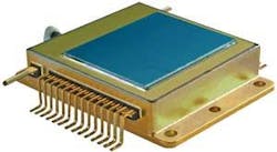
Detector manufacturer ULIS (Veurey-Voroize, France), a subsidiary of Sofradir and GE Equity, launched a fourth-generation IR detector at SPIE’s 2009 Defense, Security + Sensing conference; the XGA format (1024 × 768), 17 µm pixel-pitch sensor enables high-definition imaging for IR surveillance applications.1
The uncooled, large-format IR detector is fabricated from amorphous-silicon (Si) materials monolithically integrated onto Si CMOS substrates that contain readout integrated circuits (ROICs) patterned using standard lithography techniques. Because amorphous Si has a constant and uniform activation energy between about –30°C to +80°C, the small (less than 1%) temperature variation over this 110°C temperature range means that these detectors do not need thermoelectric cooling (see figure).
Extracting faint signals
As pixel sizes decrease, so too does the signal level that can be extracted from each pixel. The ROIC design of the 17 µm pixel-pitch detector allows integration of the microbolometer thermal signal after subtracting a common background current. This signal is then sampled and held row-by-row and multiplexed to the output. Because the ROIC requires only a 3.6 V bias signal, a low power consumption of only 140 mW is required for a 30 Hz video output. The row-by-row pulse-biased pixel array can be read at faster frame rates with a reduced image format, and the image can be read horizontally or vertically.
Typical imaging tests show a mean responsivity value of 15.5 mV/K with available dynamic range higher than 100°C due to the high responsivity uniformity that characterizes amorphous Si technology. Pixel-defect rates are typically less than 0.5% for a 1024 × 768-pixel detector, similar to Si CMOS sensors developed for digital still-camera applications.
ULIS’ experience in developing various uncooled IR focal-plane arrays with pixels ranging from 45 to 17 µm in size has shown that incremental improvements in photolithography resolution, which result in smaller feature sizes, do not compromise detector fill factor. In fact, gains in photolithographic resolution allow size reduction of certain patterned features that can offset the reduction in optical collection area due to smaller pixel sizes and the subsequent increase in noise. For example, an uncooled IR pixel is composed of an absorber and a thermometer (made from amorphous Si), both integrated on top of a CMOS readout circuit. To ensure a large temperature shift of the absorber when it absorbs IR light, the electrical contacts to the thermometer that support the suspended structure have to be thermally resistive. One possibility to increase the signal is to increase the thermal insulation of the absorber by controlling the patterned features through lithography improvements.
In the future, the company plans to extend the 17 µm pixel pitch to a smaller-format 640 × 480 array, and then 320 × 240 and 160 × 120 arrays, allowing fabrication of a larger number of dies per wafer with reduced chip cost. “Since amorphous-silicon technology is based on standard microelectronics and uses the same equipment and processes, it enables high-volume production, plus an ability to reduce pixel pitch size,” says Jean-François Delepau, managing director. “We’ll continue to push the decrease in pixel size, whose limit will be the result of a tradeoff between system sensitivity, size, complexity, and cost.”
REFERENCE
- C. Trouilleau et al., SPIE Defense, Security + Sensing 2009, Orlando, FL, paper 7298-25, (April 13, 2009).

Gail Overton | Senior Editor (2004-2020)
Gail has more than 30 years of engineering, marketing, product management, and editorial experience in the photonics and optical communications industry. Before joining the staff at Laser Focus World in 2004, she held many product management and product marketing roles in the fiber-optics industry, most notably at Hughes (El Segundo, CA), GTE Labs (Waltham, MA), Corning (Corning, NY), Photon Kinetics (Beaverton, OR), and Newport Corporation (Irvine, CA). During her marketing career, Gail published articles in WDM Solutions and Sensors magazine and traveled internationally to conduct product and sales training. Gail received her BS degree in physics, with an emphasis in optics, from San Diego State University in San Diego, CA in May 1986.
