CMOS DETECTORS: Concentric photodiode array enables spatial-domain multiplexing
SYED H. MURSHID and JAMIL IQBAL
Research efforts to convert light into electrical signal have produced a wide variety of commercially available photodetectors. In the past, much of this work has been driven by the telecommunications industry, for which investment of capital was not a major issue. This led to expensive technologies that were confined to the telecommunications infrastructure. But optical engineers are increasingly turning to the low-cost, high-performance semiconductor industry model to create inexpensive devices for generating, guiding, controlling, and detecting optical signals. Meanwhile, electronics engineers are looking to optics to overcome the limits imposed by copper at high data rates and in submicron-chip-based systems designed to process large amounts of data.
Standard CMOS (complementary metal-oxide semiconductor) processing offers excellent optical properties to satisfy the needs of both groups. The technology has benefited from billions of dollars of R&D investment and a decades-long track record of innovation. Recognizing the tremendous research opportunity of CMOS and its cost benefit, we recently developed a novel array of concentric photodiodes to detect and demultiplex spatially multiplexed optical signals using silicon photonics.1 We call this development spatial-domain multiplexing (SDM) and believe it is a significant step toward creating optical building blocks using commercial CMOS processes. We also think efforts like this will spur the evolution of monolithically integrated optoelectronic systems.
CMOS photodiodes
Simply stated, a photodiode is a device that converts light (photons) into electric current (electrons). The electrical and optical properties of a p-n junction and the associated depletion layer play a central role in the functioning of a photodiode. A p-n junction is formed when p-type (positive) and n-type (negative) semiconductor materials come in contact with each other during a monolithic fabrication process. The depletion layer is created by a recombination of electrons and holes, which meet each other in their random motion around the p-n junction. As a layer is being depleted of free electrons and holes around the p-n junction, excess fixed charges are left behind: positive donor ions at the n-type side and negative acceptor ions at the p-type side. These charges create a field at the p-n junction that consequently blocks any further transport of the electrons from the n-type side into the p-type side—and vice versa. The depletion layer has a constant width when the steady state is achieved.2
Photodiodes are typically used in the reverse-bias region. In the dark, only the leakage current flows in the reverse-bias region. When exposed to light, the reverse current of the photodiode, called photo current, increases proportionally to the light intensity. The photo current does not depend on the reverse-bias voltage. Several research groups have reported successful implementations of both individual photodetectors and complete optical receivers using CMOS technology.3–5 Standard CMOS technology offers three types of p-n junctions (see Fig. 1).
The concentric design
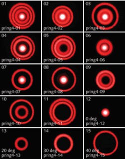
The invention of SDM makes it possible to increase the capacity of existing optical links many times over.6–8 The technique spatially multiplexes multiple optical signals (channels) of the same wavelength so they copropagate over a single strand of optical fiber. These channels follow helical paths in the fiber and each channel is confined to a dedicated radial distance from the center of the fiber. The center-most channel generally exits the output end of the fiber in the form of a spot, while the outer channels appear as concentric rings (see Fig. 2).We designed six different structures using two variations of each of the three available p-n junctions. While we had hoped to create structures composed of concentric circles, limitations imposed by both CAD tools and the preferred semiconductor foundry processes forced us to use concentric octagonal structures. The six designs were as follows:
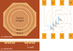
- n-well p-well (NWPW). In a design based on the n-well to p-substrate p-n junction, we used the octagonal rings of the n-well region to create concentric photodiodes (see Fig. 3).
- n-well p-well (NWPW-B). An alternate approach followed the n-well to p-substrate setup. A scheme of a central square n-well island encircled by a couple of square ring-shaped n-well islands forms this triple channel photodetector. The p-n junction still follows the n-well to p-substrate format, but the actual geometrical layout is different from the NWPW design described above.
- n-plus p-well (NPPW). This layout consists of a central octagonal n-plus region surrounded by three octagonal n-plus rings in the p-substrate. p-plus octagonal rings serve as p-substrate contacts. This arrangement forms a concentric photodetector to detect up to four SDM channels.
- n-plus p-well (NPPW-B). In this scheme we created three separate islands of p-substrate using 3-µm-thick square rings of n-well region. An n-plus octagon in the central p-substrate island forms the central photodiode. n-plus octagonal rings in the surrounding p-substrate islands form the other two concentric photodiodes. The geometric size and spacing is also different from that of the NPPW structure, above.
- p-plus n-well (PPNW). This layout involves a central octagonal p-plus region surrounded by three octagonal p-plus rings in the n-well. n-plus octagonal rings serve as n-well contacts. The result is a concentric photodetector able to detect four SDM channels. The structure is exactly same NPPW, but with n and p switching positions.
- p-plus n-well (PPNW-B). For this structure, we created three separate isolated sections of n-well. With an octagonal photodetector in the central n-well and octagonal ring detectors in the surrounding n-well islands, this arrangement constitutes a set of three concentric optical detectors.
Measurements and results
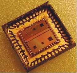
The measurements taken on the packaged parts showed very encouraging results. All the devices are functional and generate reasonable responsivity. In this initial design our effort was focused on proving the concept while staying within the constraints of a standard CMOS process. Most measurements generated results close to the expected value of 0.45 A/W for the wavelength used (660 nm).
Responsivity of central octagonal photodiodes for NWPW, PPNW, and NPPW structures fell close to the expected values. Similarly, the concentric octagonal photodiode Ring 1 and Ring 2 values for the same structures fell within 10% to 15% of the expected silicon responsivity at this wavelength. However, some values appeared to be a little high, and we are currently investigating this. Some of these outliers could be attributed to the process variations. High leakage currents across the concentric structures and certain parasitic p-n-p or n-p-n structures may also be responsible for high responsivity. This can be avoided in future designs through precise selection of well spacing and well pickup contact locations, and using a triple-well process to achieve better inter-ring isolation.
By successfully implementing our design in a standard CMOS process we achieved our primary goal of identifying an enabling technology for SDM. The concept demonstrated in silicon can be easily extended to other materials suitable for optical communications. This also demonstrates that CMOS photonics could be used in innovative ways to accomplish optoelectronic tasks in an effective and efficient manner.
ACKNOWLEDGMENT
The authors would like to extend their gratitude to MOSIS Education Program (MEP) and the associated team for their support. The MEP is playing a vital role in providing university researchers a platform that translates concepts into practice. This makes MOSIS a significant contributor to research, development, and innovation. This endeavor might not have been possible without support from MEP.
REFERENCES
- S. Murshid et al., “Method and apparatus for spatial domain multiplexing in optical fiber communications,” US Patent 7,174,067.
- S. Dimitrijev, Understanding Semiconductor Devices, ch. 2, New York: Oxford University Press (2000).
- H. Zimmermann et al., IEEE Photon. Technol. Lett. 11, p. 254 (Feb. 1999).
- C. Rooman et al, IEEE J. Solid-State Circuits 35(7) (July 2000).
- T.K. Woodward and Ashok V. Krishnamoorthy, IEEE J. Sel. Topics in Quant. Electronics 5(2) (March/April 1999).
- S. Murshid et al, J. Optics and Laser Tech. 40, p. 1030 (2008).
- S. Murshid et al, Conference on Lasers and Electro-optics (CLEO), JWA 2008;107.
- S. Murshid and A. Chakravarty, J. Optical Engineering 47(10) p. 105002 (2008).
- S. Murshid and J. Iqbal, Frontiers in Optics (FiO) 2008/Laser Science XXIV (LS) Conf. FiO/LS, OSA Technical Digest (CD) (Optical Society of America, 2008), paper FTuU6, (2008).
- S. Murshid and J. Iqbal, Elsevier J. Optics and Laser Technology (2009), DOI: 10.1016/j.optlastec.2008.12.013
Syed H. Murshid is a professor and Jamil Iqbal is a doctoral candidate in the Department of Electrical and Computer Engineering at Florida Institute of Technology, 150 West University Boulevard, Melbourne, FL.; e-mail: [email protected].


