CMOS Sensors: CMOS and CCD combine in NIR time-of-flight on-chip imager
BEAT DE COI and STEVEN FREEDMAN
Over the last few decades, the imaging world has seen numerous publications on the comparison of charge-coupled device (CCD) and complementary metal-oxide semiconductor (CMOS) imaging technologies. Intense discussions and even fierce disputes about the superiority of either approach are commonplace.
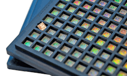
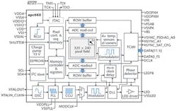
In response to this conflict, ESPROS Photonics has developed a backside-illuminated imager with a thick substrate that merges CCD and CMOS technology while improving near-infrared (near-IR or NIR) optical performance. This true system-on-chip (SoC) time-of-flight (TOF) imager enables improved time-delayed imaging (TDI) and fluorescence lifetime imaging (FLIM) outcomes (see image at the top of this page).
Conventional shortcomings
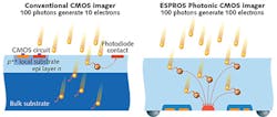
Even with commercially available CMOS image sensor (CIS) modules, standard CMOS processes are not well suited for the detection of NIR radiation. This is partially because of the fact that the thickness of the sensitive region of the pinned photodiode (PPD) is limited to a few microns—far less than the absorption length of light (about 13 μm for 850 nm light in silicon; see Fig. 1).Together, the absorption length of light for the base material, the thickness of the depleted region (plus additional diffusion region below), and the reflection properties of the surface determine the imager's quantum efficiency (QE) for a given wavelength.
The optimization of these parameters for standard photodetectors is limited by boundary conditions given by the CMOS or CCD manufacturing process. For example, the depleted region is limited by the available epitaxial thickness of commercial processes, while the optical reflection properties are defined by the back end of line (BEOL) stack that causes dominant variations on QE over wavelength because of interference patterns.
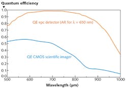
But a new mixed process from ESPROS Photonics that combines CMOS and CCD attributes addresses these limitations. The choice of a suitable substrate material contributes, among other things, to a fully depleted detector thickness of 50 μm. This results in a superior QE in the NIR region, maintaining >80% QE at λ = 850 nm and >50% QE at λ = 950 nm (see Fig. 2).CCD-CMOS integration
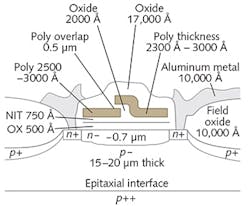
Efficient CCD implementations on standard CMOS processes need a dual poly-silicon approach to achieve a good charge transfer efficiency (CTE). The CCD gates overlap from one poly layer to the other, isolated just by a very thin oxide layer. A thin and well controlled poly layer is the key for a high CTE (see Fig. 3).However, by using size features less than 0.25 μm, dual-poly is no longer possible because process nodes starting at 180 nm and less uses a chemical mechanical polishing (CMP) process in the BEOL. CMP requires an absolutely flat surface for the layer deposition and structuring, so a second poly silicon layer is no longer possible. The key to a good CTE is a very narrow poly gap between the two gates. Such a narrow gap can be easily achieved by the use of a 45 nm (or less) process. However, because the non-recurring engineering and tooling costs (NRE) of such technology nodes are prohibitively high, they eliminate themselves as a candidate for a CCD implementation on CMOS. The ESPROS technology tackles this dilemma by a new designed manufacturing process. This new manufacturing process allows poly gaps of less than 100 nm, even in a standard 180 nm process environment.
The 50 μm fully depleted silicon detector volume is one of the key factors in this mixed-process imager's sensitivity, as its depth allows the absorption of photons that in a standard CMOS process simply pass through the thin epitaxial layer to be absorbed in the bulk substrate, where they generate waste energy as heat. Of course, with such a thick detector volume, a high-enough electrical field field is necessary to separate the electron-hole pairs and to collect the electrons under a CCD gate.
Additionally, within standard CMOS front-side imagers, the transistors are placed in the optical path on the front side of the chip. These transistors must be protected from activation by incoming photons. However, the unwanted effect of blocking these transistors is also the fact that it greatly reduces the surface area available to collect light. In this new mixed-process environment, however, the back side of the imager is used to collect light where no transistors are present. Combining the 100% fill factor achieved with this backside-illuminated process with the QE gains of the 50-μm-thick detector volume has enabled order-of-magnitude sensitivity improvements over standard CMOS.
Because the imager is backside-illuminated (BSI), a well-tailored antireflective (AR) coating can be applied to reduce the reflectivity of the detector in the desired wavelength range. And since the back-side light-entrance window is completely flat with no disruptive oxide stack, refractive filters can be deposited by using standard wafer-level processes.
These fabrication methods make it possible to apply a narrow-bandwidth filter bank to the back side of the detector, enabling ultra-small spectrometers for a variety of mobile applications. This new approach is also advantageous because of the omission of a metal stack on the entrance window, allowing large incident angles to be accepted for an improved optical design.
The enhanced QE translates directly to receiver sensitivity. From an application point of view, especially in time-of-flight (TOF) applications, improved QE can be leveraged to drastically reduce illumination power. Also, for a given optical signal strength (given illumination power), the exposure time can be reduced, making the camera system more robust against blurring effects because of moving targets as well as providing for high immunity against sunlight.
The presence of sunlight in the scene results in a direct-current (DC), non-modulated background signal that is many orders of magnitude larger than the signal to be detected. But the special properties of these CCD-CMOS pixels make it possible to eliminate the effect of DC background almost completely, which is critical for achieving accurate distance measurement using TOF in a variety of real-world environments.
The backside contacting is a process-inherent feature and all physical contacts remain on the frontside of the chip.
The best of both worlds
Although these deployed measures to optimize QE are not stringent preconditions for successfully merging CCD and CMOS features, they facilitate the mitigation of drawbacks for either technology. For example, CMOS requires additional transistors in each pixel to realize global shuttering, which usually causes a loss in fill factor and adversely affects responsivity. But in this new hybrid process, shuttering is completely implemented in the charge domain and can be controlled down to nanoseconds.
Also, repetitive shuttering with frame-store functionality in dedicated frame buffers has been realized by our design. The full CMOS analog design features, including high-voltage transistors and electrically erasable programmable read-only memory (EEPROM) blocks, remain available for the pixel architecture with no compromise in fill factor. As a matter of fact, these BSI-based hybrid optical detectors can offer 100% fill factor, virtually independent of the numbers of transistors in the pixel.
The CMOS baseline process for our hybrid detector is based on a one polymer six metal (1P6M) process with a critical node width of 150 nm. This process node allows high-density CMOS design capabilities. However, even more important, the small structures allow source followers with extremely high conversion gain of up to 100 μV/e. These low-light capable and low-noise imagers are feasible for FLIM and TDI imaging.
Noise performance also greatly influences the ability to make accurate TOF measurements. When dealing with noise performance within the possibilities of a mixed-process environment, CCD pixel designs can be applied with all their noise advantages. Furthermore, in-pixel source followers do not suffer size restrictions because of BSI, and CMOS readout and amplification stages can be deployed where they deliver the best performance (such as in high-gain amplifiers).
As a further consequence, the dynamic range will profit from the ability to accumulate and handle large charge amounts, plus the degree of freedom in pixel design supports the implementation of dedicated high-dynamic-range architectures. As well, the aforementioned QE advantage plays a vital supporting role by providing higher charges that improve the noise behavior with all other factors being equal.
Specifically for TOF applications, speed is a primary requirement. Imaging speed is determined by an efficient photon conversion and the subsequent charge collection mechanisms that in turn are limited by diffusion and by drift velocities related to the levels of the applied depletion voltage. Higher depletion voltages generate stronger fields, result in faster drift velocities, and therefore faster charge separation and detection.
The implementation of CCD structures makes fast charge handling possible, enabling novel capabilities like time-gated sensors for fluorescence spectroscopy or the detection of the phase difference in a TOF system. In a TOF imager, the temporal resolution required to tackle the received signal is in the sub-nanosecond range (50 ps or less). At the same time, there is an ambient light overlay several orders of magnitude higher than the modulated illumination. Without the powerful charge separation and charge-handling engines that have been implemented in our hybrid CCD-CMOS approach, the depth resolution would be way beyond practical values or completely masked by the ambient light signal—or both.
Then again, moving one step further and looking at the speed delivered by the imaging systems, CMOS technologies have significant advantages when designing ultrafast and highly sophisticated system-on-chip (SoC) solutions.
On-chip imaging
Until now, all TOF designs lack robustness against typical environmental conditions such as background light, moving objects, and large variations in target reflectivity. In addition, these sensor devices require complicated and expensive peripheral components such as field-programmable gate arrays (FPGAs), high-speed analog-to-digital (A/D) converters, and voltage controls that result in rather bulky solutions. In the end, the size, power consumption, and cost of available cameras are still in a range that inhibits commercial use in larger volumes.
Alternatively, hybrid CCD-CMOS TOF imagers solve many of these problems. The mixed process environment has been used to create, among other imagers, a TOF system for distance monitoring that is amenable to industrial-scale applications with very different illumination and background lighting conditions.
With 64 frames/s speed parameters, the TOF SoC imager includes all necessary sub-systems, including a pixel array, analog drivers and voltage regulators, highly parallel analog-to-digital conversion, digital state machine and timing generation, high-current LED drivers, digital signal processing, and non-volatile memory to store configuration parameters (see Fig. 4).The key ingredient of the SoC is the 320 × 240 pixel quarter video graphics array (QVGA) that is capable of performing the necessary demodulation in each pixel individually by directing the signal charge in two different readout nodes according to the demodulation signal characteristics. Therefore, each pixel has two analog readout channels that are analyzed to determine the phase difference relative to the phase of the emitted light pulse.
Pixel readout uses a typical signal chain consisting of a 12-bit ADC with a signed input range from -4 to +4 V for TOF applications. The difference of two source follower outputs is sampled and can be positive or negative.
Thanks to the merger of CCD and CMOS process technologies, all known tradeoffs that formerly existed when considering one particular technology are now obsolete; indeed, better-performing optical silicon detectors in the NIR range are now possible.
Beat De Coi is CEO of ESPROS Photonics AG, Sargans, Switzerland, and Steven Freedman is managing director of ESPROS Photonics Inc., Minneapolis, MN; e-mail: [email protected]; www.espros-photonics.com.
