Advances in Imaging: Electron-initiated APDs improve high-speed SWIR imaging
JEAN-LUC GACH and PHILIPPE FEAUTRIER
In the visible spectrum, electron-multiplying charge-coupled devices (EMCCDs) improved imaging techniques—especially in the life sciences. And yet, no significant breakthroughs have been made in infrared imagery since the hybridization of III-V or II-VI semiconductors with low bandgap on complementary metal-oxide semiconductor (CMOS) read-out integrated circuits (ROICs).
The EMCCD technology permitted wide-readout bandwidths while maintaining ultralow readout noise. For example, our OCAM² camera exhibits a readout rate in excess of 132 Mpixels/s while maintaining a readout noise down to 0.1 electron.1 Up until now, no EMCCD-equivalent imagers with embedded carrier amplification existed in the infrared, neither for short-wave infrared (SWIR) imaging, nor for mid-wave or long-wave infrared (MWIR and LWIR) imaging.
Prior art
During the last few years, mercury cadmium telluride (HgCdTe) avalanche photodiodes (APDs) have been one of the most promising paths to build focal plane arrays (FPAs) for infrared low-flux and high-speed applications such as active and hyperspectral imaging.
From 2001 to 2008, numerous groups, including those led by Jeffrey D. Beck of DRS Technologies (Arlington, VA) and Marion B. Reine of BAE Systems (Lexington, MA), have reported multiplication gains of 100–1000 for low values of reverse bias—around 10 V—associated with a quasi-deterministic multiplication yielding a close-to-conserved signal-to-noise ratio (SNR) by measuring an excess noise factor F from 1.0 to 1.2.2, 3
It should be stressed that before the demonstration of F values of approximately 1.0 in HgCdTe APDs, the theoretical lower limit of the excess noise factor was considered to be F = 2.0 following a theory proposed by R. J. McIntyre of RCA Victor Company in 1966.4 The theory was based on an average impact ionization probability of the carriers and neglecting the fluctuation in the probability due to the acceleration and deceleration of the carriers in the junction.
This theory has nevertheless been successful to describe the excess noise in silicon (Si) as remarkably demonstrated for EMCCDs, where F is approximately 2.0 by Mark S. Robbins and Benjamin J. Hadwen in 2003, then at e2v Technologies (Chelmsford, Essex, England), and for III-V-based semiconductors, in which the impact ionization of both types of carriers gives the main contribution to the randomness in the multiplication and yields excess noise factors of F = 3 to 5 and avalanche breakdown at moderate gains of M < 50.5
The noise factor lower than the McIntyre limit and breakdown-free gain of HgCdTe APDs is consistent with exclusive impact ionization of the electrons, quasi-localized in space and energy due to the variations of the impact ionization probability.6 For this reason, these devices are called electron-initiated avalanche photodiodes (e-APDs).7
Electron-initiated APDs
The highest-performing e-APDs have been obtained at low temperatures (T = 77 K) in mid-wave Hg1-xCdxTe detectors with x = 0.35 to 0.3, combining high gain at low inverse bias, low excess noise factor (F = 1.2), and low dark currents. For example, Beck et al. reported equivalent input currents (shot-noise-limited input current corresponding to the output noise) of about Ieqin = 7fA with a high operability, corresponding to a current density per pixel of J = 0.44 nA/cm2 as estimated from a minimum value of NEPhmin = 0.3 at a gain of M = 946 for a λc = 4.2 μm cutoff wavelength in e-APDs at T = 77 K.
In 2008, Johan Rothman et al. at CEA/LETI and Sofradir (both in Grenoble, France) demonstrated that the equivalent input current can be as low as 1 fA in λc = 4.8 μm detectors at T = 77K for gains up to M = 100, corresponding to a rate of 6000 e-/s.8 A reduction of the dark current of several orders of magnitude is expected in higher Cd composition and heterostructure APDs.
Another exceptional feature with the HgCdTe e-APDs is a very low dispersion of the gain that enables the use of the e-APDs in imaging applications. Typically, the fluctuation in gain is considerably lower than the fluctuation in quantum efficiency. The excess noise factor (close to 1.0) of HgCdTe e-APDs makes them nearly perfect amplifiers that add no noise to the system before amplification.
In 2012, First Light Imaging’s Philippe Feautrier et al. and Gert Finger et al. of the European Southern Observatory (ESO; Garching, Germany) reported successful hybridization of HgCdTe e-APDs on CMOS ROICs with a significant number of pixels (320 × 256).9,10
Feautrier et al. also reported the use of an APD array on the ESO Very Large Telescope Interferometer (VLTI), demonstrating for the first time the successful operation of this technology in a representative environment. At that time, liquid phase epitaxy (LPE) arrays were only available. Now, manufacturers have successfully produced molecular beam epitaxy (MBE) and metal organic vapor phase epitaxy (MOVPE) e-APD diode arrays, ensuring high performance and reproducibility in the operation and quantum efficiency of these arrays with low dark current and wide-bandwidth response.
An e-APD camera
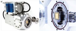
First Light Imaging is the first to make e-APD infrared array technology available in its C-RED One camera. Using a 320 × 256, 2.5 μm cutoff wavelength HgCdTe e-APD array deeply cooled to 80 K with a high-reliability pulse-tube cryocooler (mean-time between failure or MTBF of approximately 90,000 hours), the camera has a high readout speed of 1750 frames/s (full frame) while exhibiting a readout noise below one electron-thanks to the APD gain in the range of 1 to 60.
In addition to its infrared detector performance, the C-RED One camera is part of a fully integrated imaging system that operates in extreme environments and requires only an electric power supply and water cooling. No liquid nitrogen or vacuum pumping is needed for camera operation, allowing its use in remote locations without a human operator (see Fig. 1).
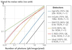
At various illumination levels, the SNR of various visible and infrared detectors is computed as:
Currently, the gain in performance of EMCCDs compared to classical CCDs in the visible is smaller than the gap between C-RED One and its competitors—whether they be slow-scan HgCdTe or even indium-gallium-arsenide (InGaAs)-based cameras. This advance in performance characteristics should allow e-APD imagers to usher in a new era in high-performance infrared detection.
REFERENCES
1. P. Feautrier et al., Publ. Astron. Soc. Pac., 123, 901, 263–274 (Mar. 2011).
2. J. D. Beck et al., J. Electron. Mater., 37, 9, 1334–1343 (Apr. 2008).
3. M. B. Reine et al., J. Electron. Mater., 36, 8, 1059–1067 (Jul. 2007).
4. R. J. McIntyre, IEEE Trans. Electron Devices, 13, 1, 164–168 (Jan. 1966).
5. M. S. Robbins and B. J. Hadwen, IEEE Trans. Electron Devices, 50, 5, 1227–1232 (2003).
6. S. Derelle et al., "A Monte Carlo study of multiplication and noise in HgCdTe avalanche photodiodes," Proc. SPIE, 7003, 70031P (Apr. 2008).
7. J. D. Beck et al., "MWIR HgCdTe avalanche photodiodes," Proc. SPIE, 4454, 188–197 (2001).
8. J. Rothman et al., "HgCdTe APD- focal plane array development at CEA Leti-Minatec," Proc. SPIE, 6542, 654219 (May 14, 2007).
9. P. Feautrier et al., "Advances in detector technologies for visible and infrared wavefront sensing," Proc. SPIE, 8447, 84470Q (Sept. 13, 2012).
10. G. Finger et al., "SAPHIRA detector for infrared wavefront sensing," Proc. SPIE, 8453, 84530T (Sept. 25, 2012).
Jean-Luc Gach and Philippe Feautrier are scientific advisors at First Light Imaging, Meyreuil, France; e-mail: [email protected]; www.first-light.fr.


