High-responsivity SiGe phototransistor is CMOS-compatible

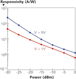
One of the most effective ways to create an integrated photodetector within a silicon photonic circuit, and to do it in a way that is compatible with standard CMOS fabrication technology, is to make the detector out of a combination of silicon and germanium (SiGe). Many versions of such a photodetector, which must be placed very close to a transimpedance and a limiting amplifier (TIA/LA), have been developed. However, the TIA/LA-based approach is expensive and takes up a lot of space. An alternate approach, that of creating a photodetector with internal gain (a phototransistor), can shrink and simplify the receiver electronics. Researchers at the Laboratory of Photonic Networks and the TeCIP Institute (both of Pisa, Italy) and University Roma Tre (Rome, Italy) have created a CMOS-compatible SiGe heterojunction bipolar phototransistor that has a maximum responsivity exceeding 232 A/W with a 45 μA dark current at a 5 V bias, and a 42 A/W responsivity with a 9 μA dark current at 1 V. The researchers have also proposed a differential-detection scheme to cancel the dark current.
The device was based on a silicon-photonics multiproject wafer run provided by CMC Microsystems (Kingston, ON, Canada). The kit (in which the circuit is designed then sent by CMC Microsystems to a foundry to fabricate) includes waveguides, couplers, modulators, and Ge photodiodes for use at 1.55 μm, but does not include phototransistors. Accordingly, the Italian researchers adapted the Ge-on-Si vertical p-i-n waveguide photodiode in the kit for their own purposes. Modifying the photodiode by adding, subtracting, and/or modifying fabrication steps, an 18-μm-long, 4-μm-wide phototransistor coupled to a tapered waveguide was the result. The fabricated device exhibited a responsivity that was highest in the microwatt range (1 μW = -30 dBm). Reference: V. Sorianello et al., Opt. Express (2015); doi:10.1364/OE.23.028163.
About the Author
John Wallace
Senior Technical Editor (1998-2022)
John Wallace was with Laser Focus World for nearly 25 years, retiring in late June 2022. He obtained a bachelor's degree in mechanical engineering and physics at Rutgers University and a master's in optical engineering at the University of Rochester. Before becoming an editor, John worked as an engineer at RCA, Exxon, Eastman Kodak, and GCA Corporation.
