INFRARED IMAGING: OLED converts IR to visible: Night vision for your cell phone?
Optical upconversion—the process of converting light at one wavelength to that of a shorter wavelength (with "up" being higher in the frequency spectrum)—is possible by directly combining photodetectors with LEDs.
Unfortunately, the fabrication process is difficult for inorganic or even hybrid organic/inorganic devices and photon-to-photon conversion efficiencies are very low—typically less than 1%. In addition, fabrication is expensive, and some alternative upconversion methods using quantum dots as an infrared (IR) absorber suffer from high dark currents. But thanks to advances in organic photodetectors and organic LEDs (OLEDs) with very high external quantum efficiencies (EQEs) on the order of 20%, researchers at the University of Florida (Gainesville, FL) have demonstrated a more efficient all-organic upconversion device that just may make night vision on your cell phone a possibility.1
All organic
The organic upconversion device, fabricated on an indium tin oxide (ITO) substrate with overall dimensions of 0.04 cm2, consisted of a tin phthalocyanine (SnPc)-based bulk heterostructure layer as a near-IR (NIR) sensitizer and an iridium-doped biphenyl OLED layer as a phosphorescent emitter—one of the most efficient OLED materials in use today. In photovoltaic mode, the EQE of the NIR sensitizer layer can be higher than 20%, while the EQE for the OLED emitter layer is close to 20% (compared to typical EQE values of less than 5% for most conventional fluorescent OLEDs).
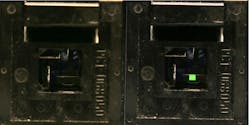
In the absence of IR radiation, the poor-hole-transport NIR sensitizer keeps the OLED layer in the off state. But upon photoexcitation, photogenerated holes are injected into the OLED layer and recombine with electrons injected from a cathode layer to emit visible light. The 100 nm thick NIR sensitizer layer or film has strong NIR absorption up to 1000 nm, with a peak at 740 nm. Using an 830 nm, 14.1 mW/cm2 NIR source, green light emission began at 2.7 V and reached a luminance of 853 cd/m2 at 15 V. At 12.7 V, the on/off ratio of luminescence intensity was about 1400 (see figure).
Even though maximum photon-to-photon conversion efficiency was only 2.7% for this device, the researchers say that this value represents an order-of-magnitude increase compared to conventional (and more expensive and complicated) hybrid organic/inorganic devices. "Since OLEDs are being used for flat-panel displays, the costs of making these organic devices are expected to be low because they can use the existing OLED manufacturing infrastructure," says Franky So, associate professor of materials science and engineering at the University of Florida.
REFERENCE
- D.Y. Kim et al., Adv. Mat. 22, 1–4 (2010).

Gail Overton | Senior Editor (2004-2020)
Gail has more than 30 years of engineering, marketing, product management, and editorial experience in the photonics and optical communications industry. Before joining the staff at Laser Focus World in 2004, she held many product management and product marketing roles in the fiber-optics industry, most notably at Hughes (El Segundo, CA), GTE Labs (Waltham, MA), Corning (Corning, NY), Photon Kinetics (Beaverton, OR), and Newport Corporation (Irvine, CA). During her marketing career, Gail published articles in WDM Solutions and Sensors magazine and traveled internationally to conduct product and sales training. Gail received her BS degree in physics, with an emphasis in optics, from San Diego State University in San Diego, CA in May 1986.
