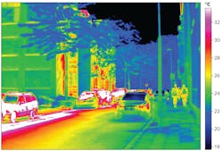
INFRARED IMAGING: Focal-plane array's hot new electronics open up 8 to 14 μm region
A way to image in a range of mid-infrared (IR) wavelengths without cryogenic cooling may become widely available thanks to efforts by scientists from the Fraunhofer Institute of Microelectronic Circuits and Systems (IMS; Duisburg, Germany). The technique concerns the long-wave IR 8 to 14 μm wavelength range–a region that normally calls for thermoelectric or liquid cryogenic cooling.
Now, Dirk Weiler of the IMS and his colleagues have shown off a completely uncooled 640 × 480-pixel IR focal-plane array (IRFPA) for the 8 to 14 μm region.1 This wavelength regime is of specific interest because it encompasses the wavelengths corresponding to the body temperature of warm-blooded animals and, crucially, humans. As a result, significant technology in both cooled and uncooled detectors exists in the military sphere in the form of night vision.
But a more prosaic–one might even say "pedestrian"–application is the detection of animals and people from, say, a moving car. Another might be in firefighting, where an appropriate IR detector might help locate people in smoke-filled buildings.
"Fraunhofer IMS has over 25 years of design experience in low-noise and low-power CMOS circuits, in particular for sensor readouts," says Weiler. "In 2006, we started the development of IR sensors with a focus on microbolometers for automotive applications." Since the early 1990s, the IMS has been developing CMOS-compatible surface micromachining, such as for capacitive pressure sensors, says Weiler. The team's IRFPA comes from this combination of electronics expertise with precision machining.
At the heart of the device is the VGA-resolution array of microbolometers, with a 25 μm pitch. These take advantage of tiny changes in resistance that the array elements exhibit when exposed to mid-IR light, turning the changes through a number of steps into a digital signal.
Resistance directly converted to digital
Normally these changes compete with IR radiation emitted by any nearby objects–hence the cryogenics. But the IMS team's array obviates the need for such cooling, largely because of a clever electronic trick in the form of a "sigma-delta" converter, which changes the way they gather a digital signal from each array element.
The conventional method is to first create an analog signal and then convert this into a digital signal using an analog-to-digital converter (ADC), says Weiler. However, the passing of the signal through the ADC adds unnecessary noise.
"The new approach is that we use a sigma-delta ADC to convert directly the resistance change of a bolometer into a digital signal," he notes. "Due to the direct conversion, we have the advantage of a better signal-to-noise ratio." Weiler says that the team has developed a complete detector device, comprising the microbolometer array, the readout circuit, and the vacuum package. The complete devices in chip-scaled packages are made on 8 in. CMOS wafers completely in-house at IMS.
Although one of the more prominent applications would be in mobile systems such as automobiles, the group is not working to integrate their detector in a full camera assembly. Instead, says Weiler, a new spin-out at the IMS will handle development and fabrication of the readout electronics, microbolometers, and vacuum package. His team, meanwhile, will work on ensuring the vacuum stability of the package as it is further refined, and improving the overall noise floor of the array.
REFERENCE
1. D. Weiler et al., Proc. SPIE, 7660; DOI: 10.1117/12.849839.
