UNIL PERERA and GAMINI ARIYAWANSA
Multimode IR detectors—which can sense different types of information from an object (or a scene) such as spatial, spectral, polarization, and temporal information—have become highly sought-after for various applications. Information from a scene in two or more spectral bands, for instance, helps to reconstruct the complete thermal profile of the scene, which can then enable identification of targets against complex backgrounds and eliminate false positives. As a complement, polarization data carries information on surface features of the target such as shape, shading, roughness, reflectivity, emissivity, and orientation, allowing a high contrast between the target and the background to be obtained.
An IR array made of multicolor (or multiband) detectors with wavelength-selection capabilities can be considered as a semiconductor or artificial IR retina, similar to the retina of a human eye, which is composed of photoreceptors sensitive to red, green, and blue light.1, 2 Such an IR retina can generate images with a huge amount of information about an object or target, mimicking biological vision. Land-mine detection, tracking and surveillance of missiles, identification of muzzle flashes from firearms, and space-situational awareness are just a few applications. In addition, multiband IR detectors can be operated as single-band detectors in each of the spectral bands.
A high-speed, voltage-selectable, multiband IR focal-plane array would satisfy most multimode sensing requirements. However, a major constraint associated with multicolor detectors is their inability to select response peaks or wavelengths without the use of optical filters and multiterminal electrical contacts on the detector. Optical filters make the detector system bulky and complicated, and reduce signal transmission as well. Detectors that have two active regions with more than two electrical contacts require sophisticated fabrication techniques. To avoid these drawbacks, one potential choice is a dual-band detector capable of bias-sensitive wavelength response.
Quantum dots and IR detectors
Semiconductor quantum dots (QDs) are nanoscale particles that have remarkable optical properties in the visible and IR regions; these properties can be controlled by changing the size of the QDs. In QD IR photodetectors (QDIPs), the electronic transitions between energy sub-bands within the conduction (or valence) band of the QDs are exploited.3 Incident IR radiation excites the electrons resting in an energy sub-band (ground state) to a higher energy state (excited state). These excited carriers can be collected as the photocurrent by applying an electrical voltage across the detector, which is a measure of the photosignal.
Although they are as well-studied as mercury cadmium telluride (MCT) detectors or even quantum-well photodetectors (QWIPs), QDIPs are expected to show several advantages, such as low dark currents and high carrier lifetimes, due to the extra degree of confinement in quantum dots.4 In addition, QDs allow normal-incidence detection, which is the primary challenge in QWIPs. The dark current of the QD structures has been further reduced using resonant-tunneling concepts.
QDIP with wavelength selectivity
A novel QD design—the superlattice QDIP (SL-QDIP)—was investigated to obtain two-color (dual-band) detection, which also allows the operator to select one wavelength band at a time using the voltage applied across the detector.5 In the IR-detector community, "superlattice" simply refers to a periodic array of closely spaced quantum wells in which the bound energy states in each quantum well couple with those in adjacent wells, forming a miniband. When QDs are placed in each well of such a superlattice, it can be referred to as a quantum-dot superlattice (QD-SL). Unlike in conventional QDIPs, the excitations of electrons from QD states to the minibands can also lead to detection. So by changing the superlattice parameters, such as the width of the quantum wells, the minibands can be shifted up or down, which allows the QD-SL to absorb radiation with different wavelengths. Hence, SL-QDIPs provide response-wavelength tunability at the detector-design stage without the need for changing the QD size.
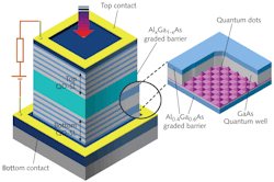
A SL-QDIP structure based on the indium gallium arsenide/gallium arsenide/aluminum gallium arsenide (InGaAs/GaAs/AlGaAs) material combination was grown by molecular-beam epitaxy (see Fig. 1). The structure consists of two QD-SLs separated by a graded AlxGa1-xAs barrier (x varies from 0.09 to 0.3), the sum of which is sandwiched between two highly doped (to a concentration of n = 2 × 1018 cm-3) GaAs contact layers. The two identical QD-SLs consist of self-assembled In0.4Ga0.6As QDs placed in a superlattice made of five periods of 90 Å GaAs/30 Å Al0.4Ga0.6As quantum wells. The pyramid-shaped QDs have a height of approximately 6 nm and a base of 20 nm, and were n-doped to 1.5 × 1018 cm-3 using silicon. Vertical circular mesas, having optically active radii of 300 µm, for top illumination were fabricated by standard photolithography, wet-chemical etching, and contact-metallization techniques. Highly doped n-type top and bottom ring contacts were formed of evaporated nickel/germanium/gold/titanium/gold with thicknesses of 250/325/650/200/2000 Å.How wavelength selectivity occurs
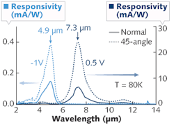
The detection mechanism and the wavelength selectivity are best understood from the conduction-band profile (see Fig. 2). The linearly graded barrier between the two QD-SLs plays an important role in terms of selecting one electronic transition at a time to contribute to the photocurrent. When a negative voltage is applied to the terminal, the top QD-SL is energetically raised to a higher level and only the electrons excited by the incident photons to the top miniband in the top QD-SL tunnel through the middle barrier, generating a photocurrent. The QD states are continuously refilled by the electron flow though the external circuit; under this condition, the bottom QD-SL stays inactive because there is no mechanism to refill the QD states after excitation. However, when a positive voltage is applied to the top terminal (forward bias), the bottom QD-SL becomes active. But the electronic transition under this condition is between the QD states and the lower miniband in the bottom QD-SL. Because the energy associated with the transitions in the reverse- and forward-bias cases are different, radiation in two wavelength bands are detected.Experimental results agree well with the theoretical explanation. At 80 K, a response band with a peak at 4.9 µm was observed for reverse bias, while a response band with a peak at 7.4 µm was observed for forward bias (see Fig. 3). Importantly, the spectral crosstalk for the two bands is low. Also, the response for radiation striking at a 45° incidence angle was higher compared to that for normal incidence. The specific detectivity—an important figure of merit indicating a measure of signal-to-noise ratio of a detector—was found to be 4 × 10¹⁰ and 8 × 10⁹ Jones at 80 K for the peaks at 4.9 µm (under -1 V bias) and 7.4 µm (under 0.5 V bias), respectively. The performance can be further improved by increasing the uniformity of the QDs.
ACKNOWLEDGMENT
This work is supported in part by the U.S. Air Force under STTR Contract FA9550-09-C-0106 and the U.S. NSF grant ECCS: 0620688. The authors acknowledge contributions from Pallab Bhattacharya's group at the University of Michigan and H.C. Liu's group at the Institute for Microstructural Sciences, National Research Council (Ottawa, ON, Canada).
REFERENCES
- A.G.U. Perera et al., Proc. World Congress on Neural Networks (1993), Lawrence Erlbaum Associates, N.J., IV.835 – IV 838 (1993).
- S. Krishna, Laser Focus World 45(3), March 2009; https://www.laserfocusworld.com/detectors-imaging/article/16551381/nextgeneration-detectors-detector-evolution-results-in-infrared-retina.
- P. Bhattacharya et al., J. Cryst. Growth 227-228, p. 27-35 (2001).
- P. Martyniuk et al., J. Appl. Phys. 104(3) p. 034314 (2008).
- G. Ariyawansa et al., Appl. Phys. Lett. 94(13) p. 131109 (2009).
Unil Perera is a professor of physics and Gamini Ariyawansa is a postdoctoral researcher at the Department of Physics and Astronomy, Georgia State University, Atlanta, Georgia 30303; e-mail: [email protected].


