AVALANCHE PHOTODIODES: Si charge avalanche enhances APD sensitivity beyond 100 GHz
KAH-WEE ANG and GUO-QIANG LO PATRICK
The development of silicon photonics has been spurred by increasing interest from the optical component community for its compatibility with existing complementary metal-oxide semiconductor (CMOS) technology. Highly sensitive photodetectors are of interest due to their potential impact on high-performance computing, data communications, consumer electronics, and medical diagnostics applications.
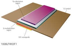
Our exploratory research team from the Institute of Microelectronics (IME) at the Agency for Science, Technology and Research (A*STAR) in Singapore recently reported the design and demonstration of a waveguide-integrated avalanche photodetector (APD) made with group IV germanium (Ge) and silicon (Si) materials (see Fig. 1).1 APDs have traditionally been fabricated from exotic compound materials using group III-V elements of the periodic table–such as indium phosphide (InP)–that are expensive and rare. In addition to high fabrication costs, the standard InP APD also suffers from degraded sensitivity because of its limited gain-bandwidth product as the data rate increases beyond 10 Gbit/s. Silicon is a familiar semiconducting material that is less prone to excess noise. In fact, Si-based APDs can offer more than 3 dB sensitivity improvement over InP-based APDs. Sensitivity in this context refers to the efficiency of the detector in converting its smallest impinging optical signal into an electrical signal while maintaining a low bit-error rate.
In addition to high sensitivity, our waveguide-integrated APD can be fabricated with CMOS-compatible processes, making it viable for high-volume production in regard to cost. CMOS technology also supports monolithic integration of passive and active photonic components that are pertinent to future microprocessor architectures in which optical communications and high-end computing are likely to converge on a single-chip platform. The waveguide configuration improves light absorption for longer-wavelength communications, extending the Ge/Si APD to a wider range of applications that require higher bandwidth.
Why group IV materials?
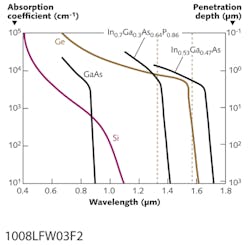
The adoption of group IV materials as an alternative to conventional III-V compound alloys for APD fabrication helps support volume economics for optical components. Ge is important because of its ability to efficiently detect incident light in the near infrared (NIR) and encode the signal into its electrical equivalent for subsequent processing. Based on the optical properties of the various group IV elements and III-V compound alloys, the high absorption coefficient of Ge makes it suitable for detecting optical signals in the standard communication wavelength regime between 1.3 and 1.55 μm (see Fig. 2). Also, the inherently good material properties of Si that allow high multiplication gain while achieving low excess noise compared to existing III-V compound alloys make it an ideal material of choice. Finally, the compatibility of group IV materials with existing CMOS process technology promises low incremental cost toward high-volume production.Overcoming technology barriers
The use of group IV materials (particularly Ge) is not without technology barriers. One of the key challenges to growing high-quality pure Ge film on Si lies with the large lattice mismatch between the two heterostructure materials. The strain from an approximately 4.2% lattice mismatch gives rise to two major issues: (1) high densities of threading dislocations near the Ge/Si interface and (2) rough surface morphology due to three-dimensional (3D) Stranski-Krastanov (SK) growth. Both of these defects can generate high leakage currents that compromise the efficiency of photodetectors.
Strategies proposed in the literature to overcome these two challenges vary. One intuitive approach is to grow a SiGe layer by compositionally grading its Ge concentration up to 100%. Using low-energy plasma-enhanced chemical vapor deposition, Oh et al. showed that for every 10% increase in the Ge mole fraction, a linearly graded SiGe buffer of approximately 1 μm thickness is required.2 This results in a need to grow a relatively thick SiGe buffer layer of 10 μm before a low-dislocation-density Ge film can be deposited, unfortunately, causing problems for process integration.
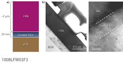
In our work, selective epitaxial growth of Ge on silicon-on-insulator (SOI) is performed using an ultrahigh-vacuum chemical vapor deposition (see Fig. 3).3 Unlike conventional approaches, a thin pseudo-graded SiGe buffer with a thickness of approximately 20 nm relieves the large lattice mismatch stress between the two heterostructure materials. The Ge mole fraction within the SiGe buffer is compositionally graded from 10% to approximately 50%. Using diluted germane (GeH4) and pure disilane (Si2H6) precursor gases, a relatively thin Ge seed layer of around 30 nm is subsequently grown on the SiGe buffer at a process temperature of 370ºC. Low-temperature growth is intended to suppress adatom migration on Si and prevent the formation of 3D SK growth, which allows a flat Ge surface morphology to be achieved. After obtaining a smooth Ge seed layer, the epitaxy process temperature is then increased to about 550ºC to facilitate faster epitaxy growth toward the desired Ge thickness. Using this approach, high-quality Ge film with a thickness up to 2 μm has been demonstrated, along with achieving a threading dislocation density as low as approximately 107 cm-2 without requiring any high-temperature cyclical thermal annealing steps.Creating and measuring an avalanche
A different type of Ge/Si photodetector with built-in amplification capability would be very useful in applications requiring high sensitivity. As the APD name suggests, an avalanche of charge occurs within the device that typically contributes to ten-fold or greater signal amplification. Our APD detector design features a separate-absorption-charge-multiplication (SACM) configuration where Ge and Si are used for light detection and charge multiplication, respectively.
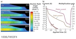
First, when the incident light illuminates the detector, a pair of negative (electron) and positive (hole) charges is generated within the Ge detection region (see Fig. 4). Due to the applied internal electric field, the electron is accelerated across the Si multiplication region until it attains a high enough energy to collide with a neighboring silicon atom to create a second pair of positive and negative charges. As the collision process continues, the number of total charges doubles to the point at which an "avalanche" of charges is generated and collected as a detection signal.Key APD performance metrics include sensitivity, charge multiplication gain, bandwidth, and dark current at operating voltage. Using conventional Ge p-i-n detectors as a reference, the primary responsivity of our device was measured to be ~0.8 A/W at unity gain. When applied bias increased, responsivity rose rapidly because carrier multiplication gain (M) enhances with increasing bias; it could reach a value as high as M = 12 when operated at 90% of the breakdown voltage. In this context, the multiplication gain factor is calculated by normalizing the APD's responsivity to the primary responsivity of a reference p-i-n detector.
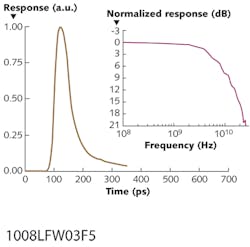
The breakdown voltage is defined at a reverse current of 100 μA, which occurs at approximately -23 V. Such high photoresponsivity is possible due to the avalanche effects that enable carrier multiplication to take place via impact ionization. When plotting the dependence of multiplication gain on the applied reverse bias at room temperature, unity gain (M = 1) occurred at the punchthrough voltage where the Ge and Si regions are totally depleted. With a further increase in the applied bias beyond punchthrough, the multiplication gain surges rapidly, contributing to sensitivity enhancement. The dark current density at punchthrough was also measured to be as low as 20 mA/cm2, showing negligible dark current degradation from an enlarged electric field strength.A 1.55 μm pulsed laser source with 80 fs pulsewidth was used to measure impulse response and determine the bandwidth performance of our APD (see Fig. 5). Devices were characterized with microwave probes and impulse response was captured using a high-speed sampling oscilloscope. When operating the device at unity gain, a maximum -3 dB bandwidth of ~7.5 GHz was achieved (the RC time constant was found to be the dominant factor limiting the speed performance). Note that the -3 dB bandwidth was obtained from the fast Fourier transform of the impulse response. When the device operates in the high multiplication gain regime, reduced APD bandwidth is observed, which is mainly attributed to the avalanche build-up time effect. For a multiplication gain of M = 21, a bandwidth performance of approximately 5 GHz was measured. This gives rise to a resulting gain-bandwidth product of about 105 GHz for the Ge/Si APD demonstrated in this work. With further device design and fabrication optimization, we expect to see a gain-bandwidth product greater than 210 GHz.
REFERENCES
1. K.-W. Ang et al., "Waveguide-Integrated Ge/Si Avalanche Photodetector with 105GHz Gain-Bandwidth Product," OFC, San Diego, CA (Mar. 2010).
2. J. Oh, S.K. Banerjee, and J.C. Campbell, IEEE Phot. Technol. Lett. 16, 2, 581–583 (2004).
3. K.-W. Ang et al., IEEE J. Selected Top. in Quantum Electron. 16, 106–113 (Jan./Feb. 2010).
