Advances in CCD technology target specific applications
The impetus for most significant developments in charge-coupled-device (CCD) technology is to address the challenges of end-user applications. As new generations of "tailored performance" detectors are implemented in increasingly creative camera designs, researchers are afforded an ever-widening array of imaging solutions. And while considerable emphasis has also been placed on CMOS development in the past few years, CCD technology continues to evolve and still represents a more appropriate choice for scientific investigation.
Low-light microscopy
Recently, CCD manufacturers introduced novel, high-sensitivity CCDs designed specifically to meet the requirements of ultralow-light imaging applications, work that heretofore had relied on camera systems equipped with image-intensifier hardware. The new detectors use revolutionary "on-chip multiplication-gain" technology to multiply photon-generated charge above the readout noise, even at supravideo frame rates. This special, signal-boosting process occurs before the charge reaches the on-chip amplifier, effectively reducing the CCD read noise by the gain factor, which generally falls between 1 and 1000. The primary benefit of the technology, therefore, is better signal-to-noise ratio for signal levels below the CCD read-noise floor.
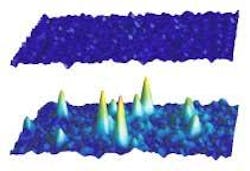
When integrated in a high-performance digital camera platform, these charge-multiplying CCDs provide an option for nongated, low-light-level applications that demand video (or supravideo) frame rates and high spatial resolution. Examples include intracellular ion imaging, biological fluid-flow measurements, and single-molecule fluorescence (SMF) imaging (see Fig. 1).
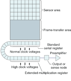
The principal difference between a charge-multiplying CCD and a standard CCD is the presence of an extended serial register (see Fig. 2). Electrons are accelerated from pixel to pixel in the extra portion of the register by applying higher-than-typical CCD clock voltages, causing ionization on impact and the subsequent generation of secondary electrons. Increasing or decreasing the clock voltages determines the on-chip multiplication gain, which is exponentially proportional to the voltage. Because the on-chip multiplication gain occurs after photons have been detected in the active area of the device, this technology is adaptable to all CCD architectures, such as back-illuminated CCDs and interline-transfer CCDs.These new charge-multiplying devices boast the sensitivity of intensified and electron-bombardment CCDs, without the risk of damage to image-intensifier hardware. Because no photocathode or phosphor is involved, spatial resolution is as high as that of standard CCD imagers with the same array and pixel size. Furthermore, the low read noise attainable with on-chip multiplication gain allows individual frames to be viewed sequentially at "live" frame rates. Low read noise also improves the capability for low-light-level work.
Fluorescence microscopy
Multidimensional fluorescence microscopy calls for imaging systems that deliver high speed and good sensitivity. Interline-transfer CCDs, in which basic architecture allows electronically shuttered fast-frame-rate operation, have followed a development path that positions them as effective, affordable devices for this application.
Standard interline-transfer CCDs suffer from relatively poor sensitivity to photons, because an opaque mask covers a large portion of each pixel. To increase a detector fill factor, high-quality interline-transfer devices use microlenses to direct the light from a larger area down to the photodiode. The microlenses collect some of the light falling on the masked area that is otherwise lost, thereby improving quantum efficiency (QE). Furthermore, microlenses increase the effective fill factor of the CCD from approximately 40% to greater than 75%.
The first manufacturer to implement interline-transfer CCDs with microlenses, Sony (Tokyo, Japan), subsequently improved the microlens technology and manufacturing process with the introduction of the hyper hole-accumulation-diode (HAD) CCD. Hyper HAD CCDs feature much tighter spacing between microlenses, further increasing the light-collection efficiency, even with reduced pixel sizes.
Sony has also developed the super HAD interline CCD, a device with an additional layer of on-chip microlenses positioned close to the pixel area. When used with fast, low-/number lenses, a single array of microlenses cannot focus the higher-angle light rays onto the active area of the pixel and sensitivity is reduced. The second layer of microlenses further condenses the beam path, thereby raising QE.
Sony took interline technology yet another step by improving the QE in the near-infrared (NIR) region with the introduction of EXview HAD CCDs. Since NIR photons are absorbed at deeper levels in the silicon, using thicker silicon in the chip increases the probability of photon-silicon interaction and thus further increases QE.
Gene-chip readers
Efficient gene-chip readers for genomics and proteomics applications depend on high throughput, a parameter determined to a large extent by the sensitivity of the imaging system used in the reader. The KAF3200ME is a CCD recently introduced by Eastman Kodak (Rochester, NY) for use in these instruments.
A few years ago, the Kodak Microelectronics Technology Division (now known as Kodak Image Sensor Solutions) developed a fabrication process that produces CCD gates more transparent to light than those used in conventional devices. Based on indium tin oxide, the "ITO" gates provide better light throughput into the photoconversion layer of the CCD. The resultant imaging devices have higher QE levels than standard front-illuminated CCDs. This improvement extends across the visible spectrum, including the blue/green region.
The superior blue/green sensitivity provided by ITO devices allows shorter exposure times because a greater amount of incident light reaches the photosensitive layer of the CCD. Thus, minimum detection levels (many assays emit in the 450- to 540-nm range) and required exposure times are lowered, resulting in better detection capabilities as well as higher throughput. The ability of ITO technology to provide higher QE without sacrificing dynamic range also allows for precise quantification.
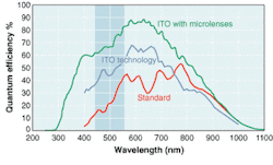
The Kodak KAF3200ME detector reaches even loftier performance heights by pairing ITO technology with microlenses in a 3.2-million-pixel full-frame device. The combination of microlenses and ITO technology has a positive synergistic effect. Used in concert, these two design features deliver the highest QE available in a front-illuminated CCD (see Fig. 3), approaching the performance of back-illuminated devices.To facilitate still greater throughput, the field of view of the new CCD provides a 1:1 optical ratio when used to image standard-size arrays. Integrating the KAF3200ME into a camera system gives gene chip readers the full benefit of the ITO/microlens technology tandem.
NIR Raman spectroscopy
At NIR wavelengths, the silicon in CCDs becomes increasingly transparent, causing the QE to decline. To preserve as much QE as possible, back-illuminated CCDs are often used for work in the NIR wavelength range.
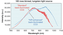
Unfortunately, reflections between the parallel front and back surfaces of back-illuminated CCDs cause them to act as partial etalons. This etalon-like behavior leads to unwanted fringes of constructive and destructive interference, which artificially modulate a spectrum. The extent of modulation can be quite significant (more than 20%) and the spectral spacing of fringes (typically 5 nm) is close enough to make them troublesome for almost all NIR spectroscopy.
The back surface of back-illuminated detectors (the surface through which light enters the CCD) is typically antireflection (AR) coated. These coatings are not perfect, however, and their effectiveness varies by wavelength. Most CCD back-surface antireflection coatings are not optimized for the NIR. A series of back-illuminated detectors developed jointly with CCD manufacturer E2V (Chelmsford, England) uses several special design features to reduce etalon effects (see Fig. 4).These customized "deep-depletion" CCDs are made of thicker silicon, roughly double the thickness of normal back-illuminated CCDs. This contributes significantly to the absorption of NIR light, reducing the amount of light that survives a round-trip path to cause interference, as well as increasing the QE. Next, the AR coating has been optimized for NIR wavelengths, reducing the amount of light reflected into the device when the light returns to the back surface from the polysilicon side. The AR coating also increases the amount of light that passes into the CCD initially, thereby increasing the QE and reducing stray light in the spectrometer. Finally, the back surface is processed to help to break up the etalon effect.
Manufacturers will continue to extend scientific imaging capabilities, resulting in burgeoning application areas and a steady proliferation of highly inventive, specialized CCDs and camera systems.
About the Author
Jeff Grant
Senior Writer, Roper Scientific
Jeff Grant is senior writer at Roper Scientific (Tucson, AZ).
Stephen Marcus
Vice President of Engineering, Roper Scientific
Stephen Marcus is vice president of engineering at Roper Scientific (Tucson, AZ).


