APD ARRAYS: Avalanche photodiode arrays provide versatility in ultrasensitive applications
NICK BERTONE and WILLIAM CLARK
In imaging applications, a two-dimensional (2-D) detector with very high quantum efficiency is desirable to optimize sensitivity. The imaging detectors of choice today are electron-multiplied charge-coupled devices (EMCCDs), not to be confused with the “avalanche process” in avalanche photodiodes (APDs). Electron-multiplied CCDs are very sensitive, and if cooled, can approach single-photon sensitivities. However, the timing resolution of these detectors is poor—on the order of milliseconds to microseconds. This is where APDs have a distinct advantage. The timing resolution of APDs can be in the picosecond range, making them orders of magnitude faster than CCDs.
Avalanche photodiodes can be operated in linear mode, in which the APD is biased below the breakdown voltage, or in Geiger mode, in which the APD operates above the breakdown voltage. A third operating region presented earlier this year, is referred to as sub-Geiger mode, in which the APD is sensitive to single photons and is biased to a very high gain of approximately 1000 but below breakdown.1 In linear mode, an APD is usually connected to an amplifier. The timing resolution of the APD and amplifier circuit is the result of the jitter of the APD itself plus that of the amplifier, and can be in the range of hundreds of picoseconds. For optimal sensitivity, the APD gain is normally set so that the noise of the APD is equal to the noise of the amplifier. In this mode, the sensitivity of an APD is better than using a p-i-n diode, but is typically limited to about 500 photons.
When operating the APD above the breakdown voltage, the APD is referred to as a single-photon avalanche diode (SPAD). The SPAD remains in an “off” state until a photon instantaneously drives the current to about 10 mA via the avalanche process. This current can be detected with precise timing, indicating the arrival of the photon. The SPAD must be reset or quenched so it can count the next photon. Silicon SPADs require 50 to 70 ns to reset, which is referred to as the reset or dead time. The key advantage of operating the APD in this mode is that it becomes extremely sensitive—capable of detecting single photons with a timing resolution of 30 ps or faster.
APD and SPAD arrays
Many applications, including time-resolved microscopy and flash ladar, would benefit from APD and SPAD arrays. In some of these applications, CCDs are used to acquire the images and a single-pixel APD or SPAD is incorporated for the lifetime or range measurement. These single-pixel detectors only provide the measurement at one point of the image. If the entire image requires these measurements, the APD or SPAD must build the image one point at a time using scanning optics.2 An APD or SPAD array would not only eliminate the need for scanning optics, it would also allow for much faster image reconstruction.
However, APD and SPAD arrays are not yet mainstream products. High-yield production of arrays is not easily achievable. Each APD has a different gain-versus-voltage characteristic and in some cases the difference can be quite substantial. This means for an APD array biased with the same voltage across the array, the gain of each pixel will be different. In addition, each pixel in the APD array will require its own amplifier circuit and the more pixels in the array, the more complex the read-out circuit. Finally, in photon-counting mode, the pixels will emit photons when they avalanche, which will trigger the adjacent pixels if they are closely packed. To reduce this phenomenon, the pixels need to be separated by a substantial distance, which will result in much lower fill-factor compared to CCDs. Despite these limitations and fabrication issues, several unique programs and projects have funded the development of APD and SPAD arrays.
3-D imaging
The rapidly emerging technology of three-dimensional (3-D) imaging requires the use of large-format indium gallium arsenide (InGaAs) avalanche photodiode arrays because of their high speed and sensitivity to eye-safe wavelengths. Until now these large-format APDs have been virtually nonexistent due to manufacturing issues related to nonuniformities in the epitaxial growth and junction formation process. A mere fraction of a percent variation in the epi-layer thickness or doping concentration results in sizable shifts in APD operating voltage that can render an array useless. This is because the silicon-based read-out integrated circuits (ROICs) with which the arrays are integrated only have about 4 V of bias adjustment available for each APD element. Arrays with nonuniformities in operating voltage of greater than 4 V are unusable, as the gain across the imaging array cannot be equalized.
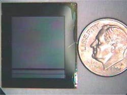
Engineers at OptoGration (Haverhill, MA) designed a 256 × 256 InGaAs-indium aluminum arsenide (InAlAs) APD array spanning more than 1.5 cm2 that has low noise, excellent uniformity and quantum efficiency, and is suitable for sophisticated flash-ladar imaging systems (see Fig. 1). All 100 APD pixels had breakdown voltages within a 2 V range and had dark-current values of less than 4 nA at a voltage corresponding to 10 A/W, or a gain of approximately 10. OptoGration has successfully manufactured arrays with dimensions of 64 × 64, 16 × 256, and 256 × 256. These arrays are very attractive for 3-D imaging flash-ladar systems used in imaging systems in autonomous vehicles, collision avoidance, terrain mapping, and remote-sensing applications.
SPAD arrays
Applications for photon-counting detectors are well established and the sensitivity and timing resolution of SPADs are far superior to any other detector technology. If a SPAD array could provide these sensitivity levels and timing resolution, they would provide tremendous value in many applications. Work in this area is progressing, with some leading research groups providing custom modules for specific applications.
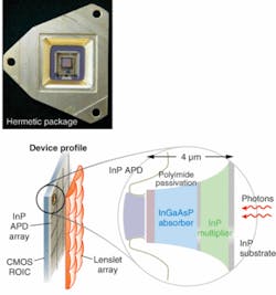
MIT Lincoln Laboratory (Lexington, MA) has developed an 8 × 8 SPAD array for operation at 1060 nm. The detector material is InGaAs-indium phosphide, which provides high detection efficiency at these infrared wavelengths. The reset time (dead time) is set at 1.6 μs, limiting the count rate to approximately 10 million counts per second aggregated across the array. The array design, leveraged earlier 3-D-ladar efforts and is being explored for efficient laser communications, in particular for deep-space laser communication systems (see Fig. 2).At Politecnico di Milano (Milan, Italy), Sergio Cova’s group has been working on photon-counting detectors and quenching circuits for more than two decades. The group developed the first single-photon-counting detector capable of 30 ps timing resolution and is working on silicon-based photon-counting arrays. One of the projects the group is working on is a 6 × 8 array for protein analysis. The pixel pitch is 240 μm and each pixel has a diameter of 50 μm. The pitch was selected to minimize crosstalk and enable use of the array with standard microlens arrays.
The key advantage of such single-photon arrays is that each pixel is independent and capable of 60 to 100 ps timing resolution. In this case, protein analysis is accomplished in a plate above the detector and then focused onto the detector by the microlens array. In the future, Cova’s group is planning to spot the molecular probes directly on the surface of the SPAD array to eliminate the need for the lens or other optics. The group is also working on a 60-element array for an adaptive-optics system for the European Southern Observatory.
Avalanche photodiode and SPAD arrays offer a distinct advantage in that they are ultrasensitive while still providing fast timing resolution. Although CCDs are capable of detecting low light levels, the timing resolution they provide is very poor. As more applications require imaging with fast timing resolution, the technology of APD and SPAD arrays will continue to develop. For now, building an image one pixel at a time using point detectors is still the preferred technique—especially for SPADs.
Acknowledgment
The authors wish to thank Massimo Ghioni for his insights and comments.
REFERENCES
1. W.R. Clark, K. Vaccaro, and W. D. Waters, Proc.Photonics North, Ottawa, Canada (2007).
2. J. Humpolickova et al., Proc. SPIE 6583, 658308 (2007).
Nick Bertone is president of OptoElectronic Components, 28 Des Lilas, Kirkland, QC, Canada, H9J 4A7; e-mail: [email protected]; www.optoecomponents.com. William Clark is an electrical engineer at OptoGration, 1429 Hilldale Ave., Haverhill, MA 01832.

