SILICON PHOTONICS: Monolithic optical receiver has integrated Ge photodetectors

In personal computers, the arrival of a “breakthrough” technology is never a surprise. For example, work on optical-disc recording began more than a decade before CD drives came into general use on PCs in the early 1990s. Now looms another leap forward: that of silicon photonics. While years will pass before such technology is featured at the local computer store, it is already close to practical use for supercomputing in the form of CMOS-compatible 10 Gbit/s optoelectronic transceivers under development at Luxtera (Carlsbad, CA).
One of the sticking points in creating a silicon-based transceiver is the photodetector. Silicon’s 1.1 µm band edge requires that longer wavelengths (typically 1.5 µm) be used to transmit light through a silicon waveguide, and at the same time rules out the use of silicon as a photodetector material. Germanium (Ge) is the usual replacement, in the form of a hybrid photodetector. However, fabricating separate Ge devices, aligning them to the silicon waveguides and electronics, and testing can be expensive and time-consuming.
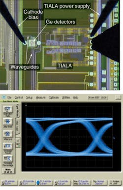
Luxtera has unveiled its own approach: a 1.5 µm detector seamlessly integrated with its receiver electronics, fabricated using the same CMOS process used to make standard computer chips (see figure). Although the detector is Ge-based, the Ge is just another thin-film layer applied in the chip-fabrication process, dropping photodetector cost to almost nothing. The devices are fabricated at Freescale Semiconductor (Austin, TX).
Making integration possible
Integrating Ge into the Freescale process involved tackling problems with geometry (solved by going with a waveguide-detector configuration rather than surface illumination), the low maximum temperature Ge could withstand (necessitating inserting the Ge after the higher-temperature processes), and others. “It was essential to develop a low-thermal-budget process that could fit into a standard CMOS flow without impacting the performance of transistors and other optical devices while providing a reasonable material quality,” said Gianlorenzo Masini, Luxtera’s chief principal scientist.
A 200 nm epitaxially grown Ge layer resulted in a detector with a responsivity of 0.6 A/W at 1554 nm, a dark current of 10 µA, and a 3 dB bandwidth of more than 20 GHz at 50°C and 1 V reverse bias. At 10 Gbit/s and an average detector power of -14.2 dBm, the complete receiver has a bit-error rate of 10-12.
Proper integration of photonics and electronics was crucial; for example, operation of the transimpedance amplifier, which is used to convert the photocurrent into a voltage signal, was improved by keeping the photodetector capacitance to a minimum, according to Masini.
Large-scale photonic integration has its benefits. “Germanium waveguide photodetectors can be tested at the wafer scale before die dicing, thanks to the optical input/output elements integrated in our technology,” says Masini. “We use a standard electronic-probe station modified to provide optical inputs, which can be continuous-wave or modulated depending on the test type. In such a way we can measure the most relevant detector parameters, such as dark current, responsivity, and speed. More important, we can test and qualify a full receiver chain using our probe station before the wafer is diced.” Moreover, he notes, the cost of hundreds or thousands of detectors in a monolithic-integration approach is identical to the cost of one.
Luxtera plans its market entry late this year, in the form of high-speed optical interconnects to replace copper wires between supercomputing units, and aims to introduce a consumer-video interconnect in 2008 at a production volume of millions of units. Further down the road are PC optical busses and multicore-processor interconnects; uses in sensors for 3-D imaging, IR, and computer gaming are also targeted.
About the Author
John Wallace
Senior Technical Editor (1998-2022)
John Wallace was with Laser Focus World for nearly 25 years, retiring in late June 2022. He obtained a bachelor's degree in mechanical engineering and physics at Rutgers University and a master's in optical engineering at the University of Rochester. Before becoming an editor, John worked as an engineer at RCA, Exxon, Eastman Kodak, and GCA Corporation.
