The invention of the transistor in 1948 ranks as a seminal event of technology. Its influence swept over the electronics industry like a tsunami, leaving in its wake portable TVs, pocket radios, and the virtual demise of vacuum tubes. But the real electronics revolution came in the 1960s with the integration of transistors and other semiconductor devices into monolithic circuits. Now integrated circuits can be found in everything from wristwatches to automobile engines and are the driving force behind the personal-computer boom.
But the last 30 years also have brought us to the brink of another technological revolution: optoelectronic integration. Materials science and advanced fabrication methods such as molecular-beam epitaxy, metal-organic chemical vapor deposition, and focused-ion-beam micromachining have enabled optical, electro-optic, and electronic components to be consolidated into monolithic structures. Integration of these normally disparate elements allows designers to combine the advantages of each in a single device.
However, optoelectronic integration does not come without effort. The proximity of such widely disparate elements on a single structure or wafer often leads to intractable incompatibilities between materials. Interference or crosstalk between various elements also can hamper the performance of the final device. Nevertheless, a number of successful strategies have been developed to deal with these and other problems; this article discusses some of them.
One of the best examples of an optoelectronic integrated circuit or OEIC is the active-matrix LCD, which already has been described in this series (see Back to Basics, Oct. 1995, p. 121). Active-matrix LCDs are large-scale OEICs in which thousands of electro-optic spatial light modulators are integrated with thousands of transistors into a large array. But other forms of optoelectronic integration are possible, too. These include various types of diode lasers (or LEDs) and their drive electronics; photodetectors and their amplification circuitry; switches, modulators, couplers, waveguides, and optical components; and all of, or combinations of, the above.
OEICs with lasers
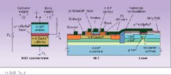
The need for cheaper, faster, smaller fiberoptic transmitters has stimulated a great deal of research into the optoelectronic integration of diode lasers and their drive electronics. Figure 1 illustrates a simple example of this kind of integration, a device that combines an AlGaAs buried-heterostructure diode laser and two metal-semiconductor field-effect transistors (MESFETs) on a single substrate. The purpose of the MESFETs is to control the current flow to the laser. One transistor supplies a bias current to keep the laser above threshold, while the other provides a modulation current for direct modulation of the laser output. Both currents are separately controlled by voltages applied to the MESFET gates (gates 1 and 2 in the figure).
Closer inspection of the MESFET structure reveals that it consists of a single layer of n-type GaAs grown on a semi-insulating GaAs substrate and capped with three separate metal contacts that serve as the source, gate, and drain of the transistor. If the source is connected to ground and a positive voltage is applied to the drain, current will flow between the two contacts via the n-type GaAs layer, which serves as a channel. However, if a negative voltage is applied to the gate, the reverse bias will create a depletion region in the n-type channel below the gate, which will impede current flow between the source and drain. In fact, if the gate voltage is high enough, current flow can be completely pinched off.
When the MESFETs are integrated into the OEIC, a heavily-doped n-type layer (n+-GaAs in the figure) is grown on top of the n-GaAs channel layer to help connect the drain electrode with the n-AlGaAs stripe directly below the active region of the laser. The rest of the laser structure is grown on top of the n+-GaAs layer as shown. The laser of this OEIC can be modulated at frequencies up to 4 GHz.
One of the disadvantages of this particular OEIC design, however, is its nonplanar profile, which limits the smallest feature size attainable by photolithography. Since smaller features usually lead directly to speedier electronics, planar architectures are more desirable. To achieve this with the above OEIC, a trench can be etched into the substrate at the location where the laser is to be grown. Then when the thicker, more-complex laser structure is fabricated, its uppermost layers will lie at roughly the same height as the top layers of the transistors.
The integration of diode lasers and MESFETs has been a very successful approach to OEICs based on GaAs semiconductor compounds. Dozens of designs have evolved that take full advantage of the high electron mobility in gallium arsenide for high-speed optoelectronic devices. Moreover, the good lattice match between AlGaAs and GaAs avoids many of the problems associated with material incompatibilities. But, diode lasers based on AlGaAs/GaAs architecture emit light in the 800-nm region of the spectrum, which is fine for CD-ROMs and first-generation fiberoptic transmitters but does not address the needs of second- and third-generation fiberoptic communications at 1.3 and 1.55 µm.
Long-wavelength design
Diode lasers with outputs in the 1.3- and 1.55-µm regions are usually constructed from narrow-band-gap quaternary compounds of InGaAsP grown on InP substrates. Unfortunately, MESFETs constructed from these same materials suffer from high gate-leakage currents brought on by the lower Schottky barrier. As a result, InGaAsP/InP systems benefit from different transistor designs for optoelectronic integration.
Figure 2 illustrates the integration of a buried-heterostructure laser with three heterojunction bipolar transistors (HBTs) in an InGaAsP/InP system. The cross-sectional view shows the construction of the laser and one of the HBTs. Unlike MESFETs and other field-effect transistors that function with a horizontal geometry, HBTs have a vertical geometry consisting of an emitter, base, and collector arrayed in a stack. The n-doped emitter layer is made of a wider-band-gap material (n-InP) than the p-doped base (p-InGaAsP) and n-doped collector (n-InGaAsP).When the layers of the HBT structure are connected as shown, a forward bias is created across the base/emitter heterojunction while the collector/emitter homojunction experiences a reverse bias. The resulting current that flows through the base/emitter junction draws electrons into the thin base layer, where they are attracted to the higher positive voltage on the collector. Thus, a relatively small current flowing through the emitter/base circuit generates a much larger current through the emitter/collector circuit via the base. Therefore, modulating the emitter/base current of the HBT modulates the current through the laser, which is connected to the HBT’s collector in the OEIC.
HBTs work very well in OEICs based on the InGaAsP/InP system, and their vertical geometry and high-speed performance also are well suited for the high-density integration of wide-bandwidth fiberoptic communications devices. But certain field-effect transistor designs have proved valuable for InGaAsP/InP OEICs, too. These include metal-insulator-semiconductor field-effect transistors (MISFETs), high-electron-mobility transistors (HEMTs), and modulated-doped field-effect transistors (MODFETs).
A number of different diode-laser designs have been successfully integrated into OEICs, as well. Although buried-heterostructure and other stripe-geometry lasers with Fabry-Perot cavities work fine in an integrated environment, the cleaved or etched mirror facets can complicate the fabrication process, and the comparatively high threshold currents can cause heat-related problems with other components of the OEIC. A better solution is to use DFB or DBR lasers with low-current quantum-well gain structures. Low-current vertical-cavity surface-emitting lasers (VCSELs) also are ideal for high-density OEICs. Many examples of OEICs using these laser types can be found in the literature.
OEICs with photodetectors
Equally important for high-speed fiberoptic communications, of course, are integrated optoelectronic receivers that combine photodetectors with electronics for amplification and signal processing. Two photodetector designs are particularly suitable for OEICs: the p-i-n photodiode and a relatively recent (1980) design known as the metal-semiconductor-metal (MSM) photodiode. Both of these quantum detectors have very-high-speed performance capacity. (For a fundamental review of quantum detectors, see Laser Focus World, October 1994, p. 93.)
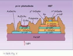
Figure 3 depicts a p-i-n photodiode and an HBT grown on a single substrate of InP. This device is an example of a vertically integrated OEIC in which all of the semiconductor layers that define the various OEIC components are first grown as a single vertical stack then selectively etched away to isolate distinct components. In this particular OEIC, the photodiode layers are laid down first, followed by the HBT layers. Selective etching then sculpts the photodiode and transistor out of the stratified composite, after which the contacts are deposited. Finally, an insulating volume of polyimide is laid down to help attenuate stray currents between the detector and transistor. Electronic interconnections between the two components are made by separate metal depositions.OEICs can be horizontally integrated, too. With this method, the stacked layers of various components are separately grown at different locations on the substrate. However, horizontal integration can create OEICs with decidedly nonplanar profiles because the thicknesses of various integrated components can vary considerably. For example, in order to achieve acceptable responsivity in a p-i-n photodiode, the light-absorbing layer must be grown rather thick. HBT layers, on the other hand, are relatively thin.
One solution, of course, is to etch a trench, or well, in the area where the photodetector layers are to be grown, as was earlier described with the laser-based OEIC. Another solution is to sink the thicker photodetector layers into previously grown layers using ion-implantation or diffusion techniques. The most direct solution, however, is to use a photodetector with a horizontal geometry. And this is one of the key features of MSM photodetectors.
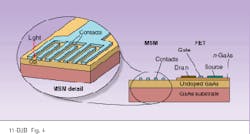
Figure 4 shows a cross-sectional view of a MSM photodiode integrated with a MESFET in a GaAs system. The MESFET consists of a channel layer of n-doped GaAs grown on a layer of undoped GaAs and capped with source, gate, and drain contacts. The enlarged perspective of the MSM region of the OEIC reveals a unique pattern of metal contacts deposited on a light-absorbing layer of undoped GaAs. In this view, the MSM structure is actually cut in half, and the front surface defines the cross-sectional plane of the OEIC. The whole OEIC structure rests on a substrate of semi-insulating GaAs.The contacts of the MSM photodiode form two interdigitated, fork-shaped electrodes that function as back-to-back Schottky diodes. When the electrodes are biased at potentials of 2 or 3 V, the GaAs region between them becomes depleted and the structure behaves like a p-i-n photodiode. Separation between the "tines" of the forks is only about 2 µm.
Besides their convenient horizontal geometry, which makes them excellent optoelectronic companions for field-effect transistors, MSM photodiodes also have extraordinarily high frequency response due to their negligible capacitance. In fact, receiver bandwidths of more than 18 GHz are possible with these devices, making them ideal for high-speed fiberoptic communications. However, because they rely on Schottky-barrier physics, conventional MSM photodiodes do not work well in narrow-band-gap systems such as InGaAs/InP. Moreover, the quantum efficiency of these detectors is diminished by the opaque metal electrodes that shadow portions of the absorbing layer.
Paths to full integration
In addition to controlling the flow of electrons between different components, OEICs also must control the flow of photons. Many strategies have been developed to accomplish this, but if semiconductor materials are used to control photon flow, the technique is generally referred to as photonic integration; if dielectric materials are used, it is called optical integration.
Both forms of integration already have been tacitly introduced in this article. The spatial light modulators of active-matrix LCDs, for instance, are examples of optical integration, while index-guided Fabry-Perot diode lasers and DFB lasers are examples of photonic integration.
In both types of integration, waveguides often play a crucial role in routing photons from one point to another on the OEIC, and a number of structures have evolved for different applications. Four common waveguide structures are the strip, embedded-strip, ridge, and strip-loaded. These waveguide structures are often completely buried beneath other layers, too, such as in the buried-heterostructure laser. All of these structures can be fabricated into a variety of geometries for different OEIC functions such as straight-line links, offset links, beam splitting and combining, and wavefront interference and coupling.
If the waveguide is accompanied by an active element such as a gain source, absorption medium, or electro-optic device, it is called an active waveguide. Simple transparent waveguides are known as passive waveguides. The combination of active and passive waveguides on a single OEIC is what enables full optoelectronic integration.
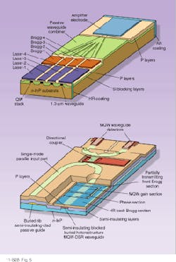
Two OEICs designed for fiberoptic communications incorporate both active and passive waveguides for full integration (see Fig. 5). The first OEIC functions as a tunable transmitter for wavelength-division-multiplexing (WDM) at four distinct wavelengths in the 1.3-µm spectral region (Fig. 5, top). It consists of four integrated multiple-quantum-well (MQW) DBR lasers linked by four passive waveguides to a MQW optical-output amplifier. Separately controlled electrodes deposited directly over the laser structures are used for both wavelength tuning and direct intensity modulation. The four passive waveguides then combine the outputs of all four lasers into a single active waveguide that passes through the MQW amplifier region. An electrode deposited above the amplifier section controls the gain of the four-wavelength output.The second OEIC (Fig. 5, bottom) functions as a balanced heterodyne receiver for coherent fiberoptic communications. It consists of passive, buried-rib waveguides, a directional coupler, two MQW photodetectors, and a MQW DBR laser as the local oscillator.
To adjust the wavelength and phase of the local oscillator for proper heterodyning with the incoming light signal, the MQW laser is equipped with separately controlled Bragg-reflector and phase sections. Wavelength tuning is accomplished by varying the voltage to the electrode deposited over the front and back Bragg reflectors. The resulting electro-optic shift in the refractive index of the Bragg gratings changes their operating wavelength. Similarly, a voltage change to the electrode over the phase section of the laser changes the refractive index of the buried waveguide and hence the phase of the wavefront passing through it.
Light from the local oscillator and input signal are mixed at the directional coupler, which is electro-optically controlled by another electrode. Buried waveguides then shepherd the heterodyned light signal from the coupler to the two photodetectors, where it is converted into an electrical signal for further electronic processing.
These devices only hint at the potential versatility of fully integrated OEICs. As fabrication and mass-production difficulties are overcome, OEICs will become essential for the high-speed fiberoptic transmitters, receivers, transceivers, and network interconnects of the information superhighway.
But the inherent parallelism, noise immunity, and speed of OEICs also make them attractive solutions for many other applications such as flat-panel displays and optical storage. For example, many commercial CD players now incorporate fully integrated optoelectronic read heads, complete with diode lasers, beamsplitting gratings, Fresnel focusing optics, waveguides, and photodetectors.
Perhaps most exciting of all is the explosive impact that OEICs will have on optical computing. The next generation of computers will rely heavily on two- and three-dimensional integration of bistable photonic switches, logic circuits, and massively parallel optical interconnects. These and other optical-computing technologies will be outlined in the next, and last, article of this Back-to-Basics series on electro-optics.
FURTHER READING
M. Dagenais et al., eds., Integrated Optoelectronics, Academic Press, San Diego, CA (1995).
O. Wada, ed., Optoelectronic Integration: Physics, Technology, and Applications, Kluwer Academic, Boston, MA (1994).
K. J. Ebeling, Integrated Optoelectronics, Springer-Verlag, Berlin, Germany (1992).
M. Razeghi, ed., Optoelectronic Materials and Device Concepts, SPIE Optical Engineering Press, Bellingham, WA (1991).
A. Selvarajan et al., eds., Optoelectronics: Technologies and Applications, SPIE Optical Engineering Press, Bellingham, WA (1993).
Thomas V. Higgins | Contributing Editor
Thomas V. Higgins was a contributing editor for Laser Focus World, covering science and technology.


