BRIAN BENAMATI
Pixel count is an important criterion in the digital still camera (DSC) market. Increasing the number of pixels provides better resolution, clarity, and the ability to print out large-format images. However, the benefits of higher-resolution imagers generally come with the penalty of longer readout times. Each pixel in a CCD needs to be read out sequentially so the signal must stay in the CCD for some period of time. This causes the dark current (unwanted signal generated in the absence of light) to build up and degrade the overall signal-to-noise ratio of the imager. One method to decrease the dark current is to cool the sensor (dark current doubles every 7°C or so) but this isn't a viable option for a portable digital camera. Depending on the environment, the internal camera temperature could reach 50°C. Another way to reduce the dark current is to run the CCD at maximum output frequency so the charge spends less time in the device. This, however, causes higher read noise—for some applications, such as scientific imaging, users prefer to operate at slower rates.
We have addressed this problem with the 11-megapixel Kodak KAI-11000CM interline CCD by developing an accumulation-mode readout method that dramatically decreases dark current. Previously, accumulation-mode timing could only be implemented by full-frame CCDs (see "CCD basics: Full-frame vs. interline").
Full-frame CCDs
In full-frame CCDs, pixels collect light and store signal charge over the entire imager, as well as serve as the transfer mechanism to shift charge and read out each c ell of information. In contrast, interline CCD architecture features pixels that have separate areas for image capture (a photodiode) and charge transfer (a vertical charge coupled device, or VCCD).
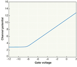
The charge packets in a full-frame CCD are moved along the shift register by clocking the gates of the CCD. The channel potential under a gate depends on the gate voltage. Above a certain voltage (in our case, it is –8 V), the channel potential has a linear dependence on gate voltage (see Fig. 2). This is the range of gate voltages at which the CCD surface is depleted of holes. Below this voltage, however, the channel potential is a constant because the potential at the surface reaches 0 V and the p+ channel isolation regions supply holes to the surface of the CCD and pin the potential at 0 V. In this condition, there are plenty of holes on the CCD surface available to recombine with electrons in surface defect levels. This dramatically reduces the surface dark-current generation rate compared to when the CCD surface is depleted of holes.1Finding the holes
Accumulation-mode readout requires a source of holes to accumulate on the surface of the CCD. Full-frame CCDs are built with an n-type buried channel in p-type substrates that acts as a source for holes. Interline CCD sensors, on the other hand, have n-type substrates, and therefore have no ready source of holes.
Actually, that isn't strictly true—there is a source for holes, but they have difficulty reaching the surface in time. Interline CCDs also have an n-type buried channel in p-doped material. The p-doped material is a well on an n-type substrate, but (unlike with full-frame CCDs) if we try to use standard accumulation-mode clocking, very few of the holes reach the surface in the center of the image sensor array quickly because of the large resistance. We could compensate for the longer times by lengthening the charge-transfer times, but that, in turn, increases the amount of dark current. The overall effect is that, for interline CCDs, standard accumulation-mode clocking results in only minor decreases in the dark current.
One of the problems that interline CCDs face is that when one of the gates transitions from –9 V to 0 V, not only are no holes able to leave the center of the image-sensor array in a reasonable amount of time, but capacitive coupling from this gate drags the p-well voltage away from 0 V. For a large-area 35-mm-format CCD such as our sensor, it could take as long as 200 µs for the p-well to return to 0 V. This phenomenon is called p-well bounce.
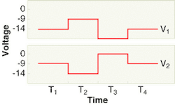
We discovered that by coordinating the voltage in the gates and the clocking, we could coax holes from one area of the surface to another, and pin the surface potential at 0 V. We solved the p-well bounce problem by placing compensating clock edges on the opposite VCCD gate (see Fig. 3). When V1 switches to 0 V, V2 has a compensating clock edge from –9 V to –14 V. When V2 goes from –9 V to –14 V the channel potential under the gate does not change because the channel surface is pinned. The effect of going further into accumulation mode is it can collect the holes from the other gate switching into depletion. This stabilizes the p-well voltage and allows fast, efficient charge transfer.At time T2, the compensating clock on V2 from –9 V to –14 V is a –5-V change while the V1 clock has a +9-V change. The –5-V change is enough to collect all of the holes from the V1 gate. The capacitance of the gate when in accumulation is larger than when in depletion so the voltage change into accumulation can be smaller than the change into depletion. The time intervals can be quite short, on the order of microseconds.
Fast readout
Another problem is that 11 megapixels provide a lot of data, and sometimes the user is more interested in speed and frame rate than in resolution. We incorporated a fast-line-dump feature that enables subsampling of rows for faster frame rates.
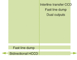
The CCD's imaging area has five times the vertical resolution required for VGA display monitors (640 × 480 pixels), so just a portion of the new sensor image area is all that's necessary to generate motion preview images quickly. While a full-frame CCD image sensor must read the entire image area to generate a photo preview, in this example the CCD can generate images five times faster.The efficiency of the fast-line-dump feature is further enhanced by dual output-mode capability (see Fig. 4). When light is converted to charge and read out by a single-output CCD sensor, each row of data is moved to a separate horizontal charge-transfer register, and charge packets for each row are read out serially—in one direction, such as left to right—and sensed by a charge-to-voltage conversion and amplifier section. In dual-output mode the device can reverse the clocking of the right half of the horizontal CCD, so that half of the data is output to the left and half to the right, effectively doubling the rate of frame generation. As a result, the camera can generate images as fast as 20 f/s—providing fluid live-motion display—and shutter speeds that far exceed the mechanical capabilities of conventional still cameras.
REFERENCE
- C. Parks and D. Losee, SPIE Proc. 5017 (January 2003).
Brian Benamati is a product-marketing engineer for image sensor solutions at Eastman Kodak Company, 1999 Lake Ave., Rochester, NY 14650; e-mail: [email protected].


