STEVEN W. MEEKS
Transparent wafers are widely used in the high-technology industry for the production of light-emitting diodes, laser diodes, surface-acoustic-wave devices, and high-power, high-temperature, and high-frequency electronics. Transparent materials used include sapphire, silicon carbide, lithium niobate, quartz, and glass. Each of these materials has its own set of characteristic defects that limit the device yield or performance. Manufacturers need to detect and classify these defects at many different stages in the construction of the devices.
Inspection of transparent wafers presents several challenges to optical-inspection capital-equipment manufacturers. One problem is that different defects can have a signature that is easily detected via one optical technique but invisible to another. For example, a hillock will be visible to an optical technique that can measure topography, but a stain will only be visible to an ellipsometer or reflectometer. Similarly, a shallow pit that may not be visible to a scatterometer can be clearly detected by an optical profilometer.
Many instruments in one optical head
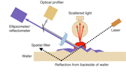
An optical surface analyzer (OSA) has been developed at Candela Instruments that solves this problem by combining an ellipsometer, reflectometer, scatterometer, and optical profiler into a single optical head. This approach enables the detection of all types of defects because it uses multiple detection methods. The OSA consists of a laser producing a beam that propagates at a high angle of incidence, allowing it to interact with the wafer substrate surface and reflecting (and scattering) from the surface. The reflected beam goes to an optical profiler, a reflectometer, and an ellipsometer channel. The scattered beam is detected via an integrating sphere. In this manner, many different types of defects can be simultaneously detected and classified. This technique has been successfully used to detect and classify pits, bumps, stains, scratches, particles, and crystal defects such as micropipes.
The optical head is mounted to a linear stage. In operation, the wafer is placed upon a rotating spindle. The wafer is rotated at a high rate of speed and the optical head moved over the surface in a spiral manner. The data from the ellipsometer, reflectometer, scatterometer, and optical profiler channels are gathered simultaneously. In this manner, the entire wafer is scanned for defects in a short period of time. Different types of defects will have different signals in each of the channels. This not only enhances the detection of the various defects, but it also allows algorithms to be developed to classify defects into the categories discussed above.
Spatial filter removes back-reflections
Light reflected from the backside of the wafer presents a significant problem in the inspection of transparent wafers. Frequently, wafers are polished only on their top surface and the unpolished backside surface creates considerable optical noise when the transmitted beam strikes the bottom surface. The OSA solves this problem by the introduction of a specially designed spatial filter to remove signals from the backside of the wafer (see Fig. 1).
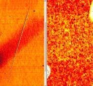
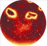
The spatial filter makes a dramatic difference in the elimination of backside noise and in the sensitivity of the system. For example, images of a scratch detected by the optical profiler channel of the OSA on a sapphire wafer can be taken both with and without the spatial filter (see Fig. 2). The image of the scratch taken without the spatial filter shows a great deal of noise from the unpolished back surface, making the scratch only faintly visible. On the other hand, the OSA image of the scratch with the spatial filter is not degraded by back surface noise; the scratch (and other features) are strongly visible.As mentioned earlier, manufacturers of electronic devices want to inspect their wafers at many points in the manufacturing process. For example, beyond the bare substrate stage, a sapphire wafer after deposition of a gallium nitride epi layer can be examined by an OSA. In this case, defects in the epi layer show up as bright spots in the reflectometer (see Fig. 3). The reflectometer image can be used to detect and count these epi defects.
Micropipes
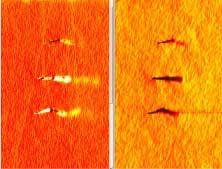
Another type of defect, which appears in silicon carbide (SiC), is a micropipe. A micropipe is a tube (with a diameter ranging from fractions of a micron to tens of microns) that propagates through a SiC crystal in the direction parallel or close to the [0001] crystallographic axis.1 The density of defects limits the applications of SiC substrates. A micropipe defect that appears in the active area of a device will destroy that device. As a result, manufacturers would like to be able to rapidly detect, count, and classify micropipes and other defects on silicon carbide.An OSA can image clusters of micropipes on SiC; both scatterometer and reflectometer images are obtained (see Fig. 4). Micropipes are actually imaged beneath the surface of the SiC. By using both the reflectometer and the scatterometer data, it is possible to uniquely identify defects as micropipes. This detection and classification capability allows manufacturers to carefully control their process and ensure that their customers are getting the quality they need.
REFERENCE
- www.marubeni-sunnyvale.com/gallium-nitride-wafers.html
Steven W. Meeks is the chief technical officer at Candela Instruments, 48890 Milmont Dr., Suite 103D, Fremont, CA 94538; e-mail: [email protected].


