HEINRICH GRÜGER, THOMAS EGLOFF, MICHAEL SCHOLLES, FABIAN ZIMMER, AND HARALD SCHENK
Hyperspectral imaging is used for a broad variety of applications ranging from the harvesting of agricultural goods to waste selection in recycling processes. In the majority of these applications, objects are transported on a conveyor belt and decisions must be made to separate items based on size or material attributes. To gather information on the shape and material composition of an object, imaging and spectroscopic data, respectively, can be used. And in the case of organic compounds, near-infrared spectroscopy is the best option.
The direct combination of imaging and spectroscopy, or hyperspectral imaging, can be applied in several configurations for inspection and sorting applications. As an object moves across a conveyor belt, diffractive elements (gratings and/or prisms) can split the light coming from the illumination system and reflected by the object into several wavelength bands. A two-dimensional detector can detect spectral and spatial dimensions, or a scanning detection system can be used for one of the dimensions in combination with a linear detector array. Because the performance of silicon-based sensors is limited for detecting light in the infrared region, more sophisticated detectors such as indium gallium arsenide (InGaAs) are often used; unfortunately, these devices are expensive—especially in linear or two-dimensional array configurations—and often preclude the use of hyperspectral imaging in price-sensitive applications. But fortunately, the use of micro-optical electromechanical systems (MOEMS) may be changing this situation.
Scanning grating technology
During the last decade, new technologies for silicon deep etching have been used to realize MOEMS that feature movable parts, such as mirror plates up to 3 × 3 mm², mounted on torsional bearings. One option to drive such devices is the use of electrostatic force through capacitors formed by comb structures on the sides of the mirror plate. The mirror plate and its bearings are physically a mass/spring system, with a specific resonance frequency, that is used for improved resonant driving of the device. This patented drive invented by Fraunhofer IPMS has some significant advantages: wide deflection angles can be reached with comparable low driving voltages.
Meanwhile scanner mirror devices realized in monocrystalline silicon are well established. Recently, the idea arose to put grating structures on the front side of the plate instead of the aluminum mirror. Today, these gratings are optimized for high-broadband throughput in the 900 to 2500 nm range (see Fig. 1).1 Our first system established with this scanning grating chip was a microspectrometer for the near-infrared spectral range.2 But to build an imaging spectrometer for hyperspectral imaging, the scanning grating chip was modified so that its tilt was across the direction of the grating structures. This modification directs the different wavelengths on the different pixels of the detector array, allowing a scan in the geometric direction with maximum resolution. For this setup, 128 to 256 pixels were desired on the detector.
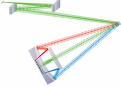
To avoid influence from lens absorption, Fraunhofer IPMS designed a completely reflective hyperspectral imaging setup.3 This so-called “Schiefspiegler optical setup” was used as starting point for optical simulations and used a 3 × 3 mm² scanning grating with 500 grooves per millimeter and 130 Hz drive frequency (see Fig. 2). Besides the completely reflective approach, this particular optical setup offers high throughput and good optical performance and resolution. The drive frequency of the grating and the geometrical resolution on the conveyor belt define the readout specification for the detector.To scan an object moving on the conveyor belt, 500 to 1000 points across the width of the belt are desired for sufficient resolution. With a 130 Hz drive frequency, this translates to a 130 kHz data collection rate, with the spectral resolution defining the number of detector pixels required. For a 1000 to 2000 nm spectral range and a resolution below 10 nm, a detector with 256 pixels is required. Unfortunately, commercially available sensors cannot meet this requirement completely, as most multipixel detectors have multiplexers on board that reduce the readout speed. Faster data access could be reached by an InGaAs detector line with parallel access to the sensor elements. An application-specific readout chip will become necessary in designs for a future product. For the test system we developed for hyperspectral imaging of objects on a 40-cm-wide conveyor belt, a multiplexed array with 20 kHz data rate is sufficient.
Plastics evaluation
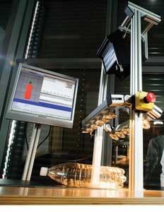
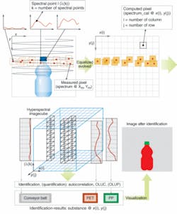
One possible application for hyperspectral imaging is the selection of plastic waste in the recycling business. Bottles of different shape and material composition have to be discriminated before recycling. A test setup was designed with this application in mind. To evaluate the physical size and chemical composition of plastic bottles on a 40-cm-wide conveyor belt, we developed a hyperspectral imaging spectrometer using nonspherical off-axis mirrors fabricated with ultraprecision milling technology and a Sensors Unlimited, Goodrich (Princeton, NJ) InGaAs detector with 256 elements (see Fig. 3). The detector data rate of 20 kHz reveals 150 points across the 40 cm belt for a geometric resolution of 2.7 mm.Spectroscopic data for each point across the belt is acquired and preprocessed by a digital-signal processor board. The spectral data is transferred to a computer by USB 2.0 and the data is evaluated spectroscopically through analytical software on the computer. In the easiest case this could be a best-match approach in which the measured spectra are compared to spectra from a material database. For more sophisticated analysis, a chemometric model for the compounds considered and specific evaluation software must be used. The output of this software process provides a material composition for each point in the sample, which could be the identification of polyethylene terephthalate (PET) for the body of a plastic bottle or just polyethylene for the cap (see Fig. 4).
Although we have used this new hyperspectral imaging system based on MOEMS scanning grating chips and analysis software to classify the plastic components of objects on a conveyor belt, the evaluation of its optical performance, spectral resolution, and possible data rate as directly correlated to the geometrical resolution and the brightness of the signal are still being optimized. Future work may include the use of two-dimensional (2-D) scanner mirrors in combination with 2-D movable scanning grating chips and a single detector. This approach would achieve the lowest possible price point, but the integration time for the detector would be extremely short and the reduced signal-to-noise ratio would need to be considered in any spectral analysis application.
Acknowledgment
This work was funded by Fraunhofer MEF program under contract number 663158.
REFERENCES
1. F. Zimmer et al., Proc. SPIE 6466, 646605 (2007).
2. Datasheet SGS 1900, www.hiperscan.com.
3. H. Grüger et al., Proc. SPIE 6887, 68870E (2008).
HEINRICH GRÜGER is sensors systems group manager, THOMAS EGLOFF is optical system design scientist, MICHAEL SCHOLLES is sensors and actuators systems business unit manager, FABIAN ZIMMER is MEMS technology development scientist, and HARALD SCHENK is micro scanner devices business unit manager, all at Fraunhofer Institute for Photonic Microsystems (Fraunhofer IPMS), Maria-Reiche-Str. 2, 01109 Dresden, Germany; e-mail: [email protected]; www.ipms.fraunhofer.de.


