A major UK collaboration has borne fruit over a range of research areas. The Multidimensional Integrated Intelligent Imaging Project (Mi3) pooled the talents from 11 research centers (see below) to advance the performance and applications of active-pixel-sensor (APS) technology. Medical applications, including mammography and portal imaging, are at the forefront of those that have benefited from the project.
Started in June 2004, Mi3 runs until June 2008 and is supported by the U.K. Research Councils through a Basic Technology Programme grant of £4.4 million (approximately US$9 million). The groups brought together in the project aimed to break the constraints of current scientific imaging in a range of applications. Advances in APS have been driven by the capability of mainstream CMOS technology—APS allows the cheaper and more flexible CMOS detectors to compete with their CCD counterparts.
The Mi3 project was established to ensure that the U.K. scientific community would capitalize on APS benefits, such as system integration, flexibility, compactness, speed, and radiation hardness. The team set out to extend the effective spectral response of APS from the visible, across the range from high-energy gamma radiation and ionizing particles, to the infrared, including the increasingly important soft-x-ray and extreme-UV regions. In addition, developing on-chip intelligence down to the pixel level was seen as a key enabler in scientific applications.
The group has had considerable success in designing and fabricating sensors and supporting instrumentation. A test structure, OPIC (On Pixel Intelligent CMOS), is designed for in-pixel intelligence, including sparse readout, analog-to-digital conversion, storage in each pixel, and setting thresholds. The CCLRC – Center for Instrumentation (see www.te.rl.ac.uk) funded the feasibility study for the OPIC sensor. Two other test structures include developments for reducing fixed-pattern noise and increasing the dynamic range (HDR) in APS.
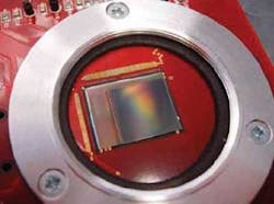
Vanilla (also known as PEAPS; see figure) is a multipurpose APS with digital and analog modes and the ability to process a “region of interest.” Operating at 100 frames/s, this sensor is a 520 × 520-pixel chip, using 25 µm pixels and with a total active area of 13 × 13 mm2. Standard CMOS detectors have good efficiency up to low-energy x-rays. Vanilla uses 150-µm-thick thallium-doped cesium iodide (Tl:CsI) as a scintillator, allowing operation with higher-energy x-rays. It has been back-thinned to increase sensitivity and is available on a ceramic header board for use in ultrahigh-vacuum systems.
Vanilla is two-side buttable. Putting units together allows a novel stitched sensor architecture that is especially useful in medical imaging. The LAS (Large Area Sensor) is due for release this spring. Other new designs include eLeNA, a test structure that develops a range of low-noise pixels. The Mi3 group also imported an existing U.K. design, StarTracker, and re-engineered it.
“At present characterization work on OPIC and StarTracker is complete, and we are continuing to characterize the other sensors,” says Catherine Clayton, project manager based at Sheffield University. “We have seen the sensors used in radiotherapy, autoradiography, and in bioarrays, among other applications. Currently we are working on variants to the instrumentation to allow the sensors to be used in electron microscopes including under ultrahigh vacuum.”
Looking to the future
“Some other designs remain more elusive,” says Clayton. “We have a list of potential sensors we would like to design and fabricate for other applications including interlaced and overlapping pixel, a flexible pixel structure with shared readouts that would enable creation of a variable pixel size. This would optimize sensitivity and resolution at a local level. In addition we would like to develop an ultrasmall-pixel APS, with pixels of approximately 2 µm, and subdiffraction-limit imaging, allowing each pixel to count incident photons with very fast readout.”
“The project has achieved a lot with new designs, including producing good detectors for high-energy x-rays,” adds Professor Nigel Allinson, also from Sheffield University. “Medical-imaging applications are really taking off. In mammography APS technology allows the use of lower doses of x-rays and faster production of results. This also extends to portal imaging and other intelligent x-ray systems, where the faster response times of APS compared with CCDs or flat-panel detectors makes real time feedback and control possible.”
Allinson says the Institute for Cancer Research (London, England) is taking the work forward into clinical trials and they expect the new sensors to find applications in astronomy and high-energy physics, but it will take longer to implement new hardware in those fields.
“There are also some exciting new developments in terms of DNA on a chip for diagnostic use; this is happening at Liverpool University [England], but IP issues mean we cannot say too much about this application,” says Allinson.
As the end of the project comes into site, what does the future hold? “Currently we are planning to continue to work together at the end of the project to pursue ideas in radiotherapy, mammography and applications in lensless electron microscopy among others,” says Clayton. “One potential area of use that we haven’t explored yet is the use of APS in synchrotrons.”
Research centers involved in the Mi3 project include the University of Sheffield, the Science and Technology Facilities Council, Brunel University, the University of Glasgow, the University of Liverpool (Liverpool Semiconductor Detector Centre and Laboratory for Environmental Gene Regulation), University College London, the University of Surrey, the University of York, the Institute for Cancer Research, and the MRC Laboratory of Molecular Biology, Cambridge. For more information about the Mi3 project see mi3.shef.ac.uk.
Bridget Marx | Contributing Editor, UK
Bridget Marx was Contributing Editor, UK for Laser Focus World.
