Microscopy Imaging: Hyperspectral microscope benefits from InGaAs imaging array
Bob Grietens
Image capture in the near-infrared spectrum at wavelengths up to 2.5 µm is becoming increasingly significant, particularly for imaging spectroscopy; for example, hyperspectral microscopes can accelerate the design process of novel LED structures.
With the introduction of indium gallium arsenide (InGaAs) as a detector material, infrared image capture is conquering ever more industrial applicationseven in cost-sensitive areas. At room temperature, InGaAs array sensors deliver good results in the near-IR up to 1.7 µm. When thermoelectrically cooled, they can be operated at wavelengths up to 2.5 µm, as an alternative to mercury cadmium telluride detectors.
Sensor-array technology
The manufacture of InGaAs sensor arrays is based on a metal-organic chemical-vapor deposition process, in which thin layers of InGaAs are deposited on substrates that have matching crystal-lattice constants, such as indium phosphide. Due to the similarity to standard silicon semiconductor manufacturing processes, this can be done at high yields in a cost-efficient way. To form the backside pixel electrodes, openings are etched into the insulating glass layer. After singulation and a functional test of the sensor chips, their pixel grids are interconnected with the readout circuitry.
Analog or digital readout circuitry, on the other hand, is created using silicon CMOS technology. Therefore, sensor-array and readout circuitry are manufactured separately and then interconnected. The interconnection method used in the InGaAs sensors made by XenICs is flip-chip bonding (bump bonding), which results in the construction of especially compact cameras. As a protective measure, the chip combination (together with an optional thermoelectric cooler) is housed in a flat package with a window of NIR-transparent glass. The module is then combined with an infrared lens, connectors, and software to form a complete camera system.
Hyperspectral-analysis technology
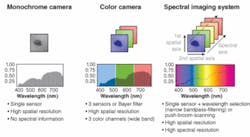
Imaging spectroscopy can be considered a happy combination of spectroscopy and image processing, and can be seen as an extension of classical image processing (see Fig. 1). In the most simple imaging configuration, a black-and-white camera captures a grayscale view of objectsat high spatial resolution, but without delivering any spectral information. A more complex arrangement consists of a color camera with either three image sensors, or one sensor with a Bayer color filter. This arrangement delivers a multispectral image at a comparably high spatial resolution plus three relatively broadband color channels; for example, red, green, and blue. However, it offers only a relatively low spectral resolution.
More complex yet are systems that capture spectral images. They work either with just one sensor and a tunable narrow-pass filter for frequency selection, or they apply the so-called push-broom scanner principle. A push-broom scannerusually via mechanical feed of either the test object or the spectrometerperforms a line scan of the object under test: for every image element in a particular line, the spectrum is captured and then stored in a pixel column of the detector. Both of these methods depend on a large number of color channelsthus the term “hyperspectral,” describing the delivery of both high spatial and high spectral resolutions. The values of the x and y coordinates of the test object and their spectral components are situated in a three-dimensional data space, or cube.
Because of their high-resolution and broadband nature, near-IR image sensors are very well suited for this sort of hyperspectral analytical equipment, which goes far beyond the mere imaging function of a camera. In a direct-view spectral camera with a grating as the dispersive element, a combination of integrated spectrograph and monochrome matrix camera basically functions as a line camera that fans out the spectrum. For each one of its linear pixels, a spectrum is generated and captured as an intensity pattern on the vertical axis (spectrum axis) of the sensor array. The horizontal axis remains the geometrical axis.
When the camera is moved, a two-dimensional image is generated, which yields properties based on its spectral intensity distribution. These can be used for classification purposes or for process control. But, unlike simply using a spectrometer, this method delivers image information as well.
Design of specialty LEDs
Often, topically relevant R&D projects act as drivers for innovations in related technical equipment. At the University of Twente (Enschede, The Netherlands), for example, researchers are investigating the impact of electrical fields on lateral LED structures by placing an additional gate electrode on top of the LED’s active light-emitting region.
Operating this LED with constant current and negative bias at the gate electrode causes it to shine brighter and the intensity profile of the radiating surface is substantially changed. Thus, the light emission of an LED can be specifically varied via a metal oxide semiconductor gate, enabling novel applications in illumination, measurement, and automation technologies.
For a thorough understanding of the underlying effects, such structures must be modeled and compared with experimental results. The more precise and meaningful these comparative measurements, the more accurate the modeling will be. Often it is not sufficient to measure just the intensity across the individual area elements: the measured intensity must be complemented by the spectral distribution of the radiation at a sufficient spatial resolution. Acquiring such data requires the approach of imaging spectroscopy.
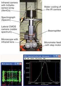
With this in mind, XenICs and the University of Twente have jointly developed a hyperspectral imaging microscope system (see Fig. 2). By means of a beamsplitter in the microscope, about a third of the emission from the LED is directed toward a laterally positioned CCD camera, which serves to align the microscope and select the object’s surface of interest. The IR camera is mounted on this structure, either directly or with a transmission spectrograph (made by the Finnish manufacturer Specim) preceding it.
The spectrograph’s dispersion element is a grating with greater than 50% transparency and a spectral resolution of 5 nm in the near-IR region from 900 to 1700 nm. The microscope’s IR lens projects the area to be measured on the test object onto the entry slit of the spectrograph. There, the incoming light is spectrally dispersed and the spatial axis, as well as the orthogonal spectral axis, are projected through an outcoupling lens onto the near-IR array sensor. This examination method is applicable to all materials and structures that can be pictured through a microscope and are somehow characterized by their spectral information.
Because of their inherent advantages of uncooled, or TE-cooled, operation, low operating cost, high sensibility, small dimensions, and high flexibility in terms of usage, InGaAs near-IR image converters enable innovative solutions in the many diverse areas of application. Thus, they are establishing new trends, as well as new benchmarks for more economical processes in design, manufacturing, process control and services.
Tell us what you think about this article. Send an e-mail to [email protected].
Bob Grietens is founder and CEO of XenICs, Ambachtenlaan 44, B-3001 Leuven, Belgium; e-mail: [email protected]; www.xenics.com.

