Photodetectors: 4th International WORKshop on Infrared Technologies highlights IR photodetector advances
On November 8-9, 2017, about 80 scientists and engineers with a stake in the infrared (IR) photonics industry gathered at Arizona State University (ASU; Tempe, AZ) for the 4th International WORKshop on Infrared Technologies, which was held for the first time in the U.S. Sponsored by Laser Components, which has manufacturing sites in the U.S. of standard and custom-made IR detectors, the WORKshop focused on IR emission, detection, and instrumentation technologies in a fast-paced, 15-minutes-per-presentation-with-embedded-breakout-poster-sessions format that visited the history of and highlighted current state-of-the-art advances in IR technology.
Specific to IR photodetection, speakers from both industry and academia described the latest advances for detectors operating in a broad range of physical environments and spanning wavelengths from the shortwave-IR (SWIR) region through the midwave-IR (MWIR) or critical chemical 'fingerprint' region and out to the longwave-IR (LWIR) region.
While advances continue to be made, nearly all the presenters emphasized that IR photodetector developers need to focus on package miniaturization, room-temperature operation, and scalable fabrication methods to address not only existing applications (also presented at the WORKshop and including atmospheric and chemical sensing, aircraft icing detection, and label-free cancer screening), but also to enable new consumer, scientific, and industrial applications.
High-speed SWIR arrays
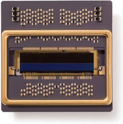
For rapid-conveyor machine-vision applications and to support increased depth penetration into ophthalmic tissue for optical coherence tomography (OCT) scanning, for example, SWIR wavelengths are ideal. But to meet the challenging requirements of high resolution and low noise for these applications, Xenics (Leuven, Belgium) has developed the XLIN-FC family of indium gallium arsenide (InGaAs)-based 12.5 μm pixel pitch SWIR linear arrays with line rates up to 400 kHz (see Fig. 1).
First introduced at LASER World of PHOTONICS 2017, the XLIN‐FC R has rectangular pixels for spectroscopy applications, while the XLIN‐FC SQ has square pixels for machine-vision applications. In both versions, the total array length does not exceed 25.6 mm.
The arrays use a modular readout integrated circuit (ROIC) design with 512 pixels that can be stitched together into 512-, 1024-, and 2048-pixel arrays. The front-end circuit is based on a capacitive transimpedance amplifier (CTIA), with input auto-zero and Correlated Double Sampling (CDS) implementation. Five gain settings are available to optimize sensitivity and dynamic range performance in a specific application.
Imaging speed for the XLIN-FC is a factor of 2.5 higher than the fastest SWIR detector currently available in the market, while keeping power consumption levels approximately the same as similar commercial devices.
MWIR lead-selenide detectors
The Laser Components Detector Group is working in conjunction with the Center for Photonics Innovation at ASU to characterize how and why lead-selenide (PbSe) IR detectors—used in the MWIR range from 1 to 4.7 μm when uncooled and up to 5.2 μm when cooled—function at the microscopic level. The company says that it is a mystery as to why room-temperature devices made by wet chemistry still outperform devices that are made with expensive deposition methods.
Initial efforts have already led to a 20% detectivity improvement for commercially available Laser Components PbSe detectors. With continued study and development, detectivity is expected to double with values approaching 5.0 × 10¹⁰ in next-generation products.
Bismuth-alloyed MWIR and LWIR progress
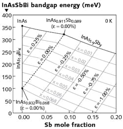
Alloying bismuth (Bi) with indium arsenide antimonide (InAsSb) on commercially available gallium antimonide (GaSb) substrates provides a material system where the biaxial strain (lattice mismatch) and photodetection cutoff wavelength (bandgap) can be independently tuned to provide an arbitrarily thick, high-quality pseudomorphic absorbing active material.1As ASU research scientist Shane Johnson explained in his IR WORKshop presentation, measurements indicate that for this composition, the strain is slightly tensile (0.055%) and the room-temperature cutoff wavelength (bandgap) is 5.7 μm (219 meV). This is substantially smaller than the room-temperature 277 meV bandgap of InAs0.911Sb0.089 lattice-matched to GaSb.
FIGURE 2. The low-temperature bandgap energy of InAsSbBi is shown as a function of Sb and Bi mole fractions; the bandgap energies decrease by about 50 meV at room temperature. Contours of constant Bi mole fraction are shown by solid curves, constant strain by dotted curves, and lattice-matched (zero strain) by dashed curves. (Courtesy of ASU)
The work by Johnson and his team indicates that alloying Bi in InAsSbBi provides a 35 meV bandgap reduction per % Bi at constant strain (see Fig. 2). That is, InAsSbBi exhibits robust absorption suitable for photodetector applications, with an absorption coefficient around 2000 cm-1 (5 μm absorption depth) near the absorption cutoff wavelength. Furthermore, the cutoff wavelength can be tuned over the technologically important MWIR and LWIR bands, covering the 3–5 μm band using dilute amounts of Bi and the 8–12 μm band using moderate Bi amounts.
Also concerning the MWIR and LWIR wavelength regions, antimonide type-II superlattices (T2SLs) such as InAs/InAs1-xSbx T2SLs have been studied for MWIR and LWIR light-emitting diodes, lasers, and photodetectors. Recently, however, Elizabeth H. Steenbergen, research electronics engineer at the Air Force Research Laboratory Space Vehicles Directorate (Albuquerque, NM), explained in her presentation that the order-of-magnitude-longer minority carrier lifetime of InAs/InAs1-xSbx T2SLs compared to that of InAs/Ga1-xInxSb T2SLs has resulted in their development for IR photodetectors, especially for space-based applications.2
MWIR to LWIR; cryogenic to HOT
In their quest to develop better cryogenically cooled single-detector elements and detector arrays for the MWIR (3–5 μm) and LWIR (8–12 μm) spectral ranges, researchers at the Fraunhofer Institute for Solid State Physics (IAF; Freiburg, Germany) focus on indium arsenide/gallium antimonide (InAs/GaSb) T2SL IR photodetectors.
Fraunhofer IAF develops T2SL array detectors for operation at 77 K and below for bi-spectral imaging in the MWIR. The combined images of two spectral ranges (3–4 μm and 4–5 μm) enable identification of carbon-dioxide exhaust—useful for missile warning systems or surveillance. In the field of cryogenically cooled photovoltaic single-detector elements for the MWIR and the LWIR, significant improvement of the signal-to-noise ratio (SNR) was achieved by dark-current reduction, realized by switching from a homojunction to a heterojunction device concept.3
WORKshop presenter and Fraunhofer IAF researcher Raphael Müller explained that widespread distribution of IR photodetectors has always been limited by the costly and complex cooling equipment needed for the highest performance, thereby motivating investigation and optimization of operation under higher operating temperatures (HOT).
To explore HOT operation, different types of photoconductive and photovoltaic detectors for the 3–12 μm spectral range were fabricated and investigated. Frontside-illuminated detectors of 1 mm diameter were grown on GaSb and small devices of 50 μm and below were grown by hetero-epitaxy on IR-transparent GaAs, allowing for backside illumination through the substrate. After formation of microlenses directly into the thick GaAs substrate beneath the photosensitive element by Fraunhofer IAF's cooperative partner VIGO Systems (Ożarów Mazowiecki, Poland), the optically active area and, therefore, the detectors' SNR was increased.
Fraunhofer IAF's development of IR detectors operated under HOT conditions is done in the framework of the MIRPHAB project initiative (www.mirphab.eu), which aims to set up a European pilot line for lasers and detectors in the IR region.
Broadband detection: SWIR to very LWIR (VLWIR)
The NASA JPL Infrared Photonics Technology Group (Pasadena, CA) has been working to improve performance of quantum structure IR detectors, concentrating on unipolar barrier designs in combination with GaSb-based alloy and superlattice absorbers that span the SWIR to very LWIR (VLWIR) spectral ranges (see Fig. 3).
FIGURE 3. An IR image taken with a JPL-developed focal plane array shows Pasadena City Hall. (Courtesy of the NASA JPL Infrared Photonics Technology Group)
Senior engineer Alex Soibel summarized his group's work in developing a LWIR complementary barrier infrared detector (CBIRD) with low dark current, an LWIR CBIRD detector with zero turn-on bias, a 320 × 256 pixel 9.9 μm cutoff wavelength CBIRD focal plane array (FPA) with a noise-equivalent differential temperature of 18.6 mK, a 1024 × 1024 pixel 11.5 μm cutoff CBIRD FPA, InAsSb-AlAsSb nBn detectors with 4.5 μm cutoff operating at room temperature, and extension of nBn detector cutoff wavelength by incorporating quantum dots into the InAsSb absorber and through an InAsSb/InSb digital alloy.4 Most recently, the JPL team demonstrated an InAsSb nBn detector monolithically integrated with a microlens fabricated on the back side of the detector (paper to be published in Applied Physics Letters).
Next-generation pyroelectric detectors
The Laser Components Pyro Group continues to advance pyroelectric (or thermal) detectors, usually targeting applications in the MWIR and LWIR regions. Its most recent advance is a patented approach using a "differential" connection method (see Fig. 4). In effect, the group has transitioned the traditional single-ended pyroelectric detector into a double-ended device, enabling a 1.4X SNR increase as well as improved EMI shielding/common mode rejection.
FIGURE 4. In a differential pyroelectric (thermal) detector, pyroelectric crystals generate positive and negative charge carriers simultaneously on opposing sides; the LD2100 series is the first series in which both crystal sides are amplified separately. (Courtesy of Laser Components)
By harnessing opposite polarities of charge on each surface of the pyroelectric material, the signals can be combined to result in the doubling of signal and a noise increase of only √2. This improvement was complemented with enhanced current mode (CM) architecture, which has led to many product variations with a 2X SNR improvement for low- to high-frequency operation. Using direct input from the CM differential into modern ADCs and microcontrollers, the signal combination can be performed in the software allowing for removal of pre-amplification stages and a decrease in developments costs.
The foregoing summaries represent only some of the presentations from the 2017 IR WORKshop. Thanks to rapid progress in IR innovation and the desire to establish closer relations between the U.S. and European IR community, Laser Components has decided to turn the WORKshop into an annual event. For more detailed information on this year's presentations and the agenda for next year at Laser Components in Olching, Germany, please contact Laser Components marketing and communications manager Myriam Gillisjans at [email protected].
REFERENCES
1. P. T. Webster et al., Appl. Phys. Lett., 111, 8, 082104 (2017).
2. E. A. Garduno et al., IEEE Trans. Nucl. Sci., 64, 4, 1042–1047 (Apr. 2017).
3. J. Schmidt et al., Infrared Phys. Technol., 85, 378–381 (2017).
4. A. Soibel et al., Appl. Phys. Lett., 109, 10, 103505 (2016).

Gail Overton | Senior Editor (2004-2020)
Gail has more than 30 years of engineering, marketing, product management, and editorial experience in the photonics and optical communications industry. Before joining the staff at Laser Focus World in 2004, she held many product management and product marketing roles in the fiber-optics industry, most notably at Hughes (El Segundo, CA), GTE Labs (Waltham, MA), Corning (Corning, NY), Photon Kinetics (Beaverton, OR), and Newport Corporation (Irvine, CA). During her marketing career, Gail published articles in WDM Solutions and Sensors magazine and traveled internationally to conduct product and sales training. Gail received her BS degree in physics, with an emphasis in optics, from San Diego State University in San Diego, CA in May 1986.


