UV DETECTORS: Silicon-rich silicon oxide films boost UV sensitivity
DAINET BERMAN-MENDOZA, MARIANO ACEVES-MIJARES, LUIS RAÚL BERRIEL-VALDOS, JAZMÍN CARRANZA, JORGE PEDRAZA, CARLOS DOMÍNGUEZ-HORNA, AND CIRO FALCONY
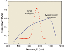
Since the discovery of photoluminescence in silicon (Si) nanocrystals embedded in silicon dioxide, much effort has been expended to take advantage of this emission. Many techniques have been used to obtain Si nanocrystals. Chemical-vapor deposition (CVD), however, is a simple way to obtain silicon-rich silicon oxide (SRO) films. This material is normally modeled as silicon dioxide that contains Si nanocrystals. It has been shown that SRO films obtained by low-pressure CVD (LPCVD) radiate intensely when they are illuminated by UV energy.1 The SRO emissions match the wavelength range in which Si is very sensitive (see Fig. 1).
The large number of potential applications has lead to great interest in developing UV Si sensors because the technology is mature and cheaper than others; however, crystalline Si photodiodes exhibit a low efficiency in the UV region (200 to 400 nm). To remedy this problem, the high sensitivity of Si in the visible can be extended to the UV region by integrating a silicon detector with an SRO film. We have developed a UV silicon detector (patent pending) made of Si and SRO that shows high efficiency and is completely compatible with silicon fabrication technology.
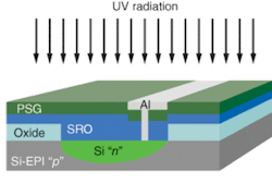
When irradiated with UV light, the SRO film in the detector emits IR and visible light that is absorbed by thep-n silicon photodetector, which generates a photocurrent proportional to the UV radiation (see Fig. 2). The main limitation of p-n photodiodes is the dark current, which defines the minimum energy detectable by the diode. In our device, a guard ring is implemented to decrease the dark current. This ring allows the reverse-polarization voltage to be increased, maintaining a low leakage current.2Silicon-rich oxide
Silicon-rich oxide is a material that shows great potential for carrying out optoelectronic functions in Si integrated circuits.3 This material can be fabricated using several technological processes: Si-implanted thermal oxide, LPCVD, and plasma-enhanced chemical-vapor deposition. In general, the substrate material is Si.
In the LPCVD process, the Si excess in the SRO film is controlled by adjusting the flow-rate ratio (Ro), which is the ratio of the quantities of nitrous oxide and silane, the reactive gases used during the growth of the film. This method produces films with diverse Si excesses; values of Ro between 10 and 30 generate Si excess in the SRO between 10% and 6%, respectively.3
After annealing at high temperatures, the SRO acquires excellent optoelectronic properties. These properties appear as a consequence of diverse effects, including consolidation and size change of Si nanocrystals, among others.
Fabrication and characterization
The substrates consisted of p-type, 10‑µm epitaxial Si wafers with a resistivity of 8 ohms-cm. After cleaning, an oxide film was grown to define a diffusion region. The oxide was etched and standard phosphorous diffusion used to form the p-n junction; the SRO was deposited over this structure. A phosphosilicate-glass film was then deposited and annealed in water and nitrogen for 30 minutes, after which aluminum contacts were etched and patterned. Finally, the devices were mounted on integrated-circuit frames.
The UV sensor was characterized with a spectrophotometer that measured over a 190- to 900-nm wavelength range using deuterium and tungsten bromide lamps. The current was measured with an electrometer. With the same setup, UV-enhanced commercial p-n diodes were measured as a comparison and to determine the source optical power.
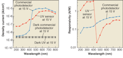
The current density and dark current of a commercial photodetector were compared with those of our UV sensor (see Fig. 3). An order-of-magnitude increase was observed in the current density of our device in the UV region (200 to 350 nm) compared to the commercial Si photodetector. Therefore, a notable improvement in the efficiency (responsivity) of the SRO detector in the UV region was observed (the responsivity for the commercial UV-enhanced diode was obtained from a curve provided by the vendor).The results clearly indicated that in the UV region the SRO-based UV detector presents a better response than the commercial one. It is necessary, however, to take into account that the numerical estimation of the responsivity (which exceeds unity in places) is obtained by comparing it with that of the commercial diode.
Two effects could produce the high responsivity observed. First, high responsivity can result from a very efficient shift from the UV to a longer, more easily detectable wavelength; therefore, the entire amount of UV-incident light could have contributed to the SRO emission. Furthermore, it is probable that light is emitted in the entire SRO film and all this light contributes to the diode photocurrent. Second, it has been observed in other studies that when SRO layers are used to produce voltage-induced p-n junctions as light detectors, high photocurrents are obtained even when the active area is covered by opaque aluminum.4 Thus, it is possible that SRO contributes in some other way to the diode photocurrent, so that an extra contribution to the responsivity has to be considered.
Applications
Many potential applications exist for sensitive UV detectors. For example, current and future optical digital storage will exploit blue and UV lasers (like Blu-ray and HD-DVD). Ultraviolet lasers emitting down to 250 nm can further increase optical-storage density; sensitive detectors will be needed for these systems.5
In the automotive industry, applications include inspecting muffler pipes for the presence of copper, detecting the presence of UV-curable gaskets, confirming the alignment of caps on connecting rods, and detecting the presence of lubricant on bearings. In packaging, UV light is used to detect the seal on ring-tab cans that prevents the seam from rusting, and is also used to detect glue on packages. In furniture manufacture, UV light helps detect the presence of excess glue in wood joints of furniture, is used to inspect the lumber for the proper coating of fungicide, and aids in controlling saws that cut wood marked with UV crayon. Other industrial uses include pharmaceutical and water treatment.
An important application of UV light is in water sterilization and food disinfection, in which it kills microorganisms. Ultraviolet technology is also suitable for use in flame detectors, fire alarms, and detection of invisible discharge phenomena such as corona discharge of high-voltage transmission lines. In addition, uses exist in health care (UV exposure measurements) and astronomy.
We are continuing to characterize the SRO-based UV sensor and improve its structure to further increase its UV sensitivity, and developing integrated structures. The Instituto Nacional de Astrofísica Óptica y Electrónica is a research institute with limited silicon-processing facilities; we are looking for a commercial producer interested in transferring this technology to the marketplace.
ACKNOWLEDGMENTS
The authors wish to thank Pablo Alarcon for the sample preparation and Jacobo Ramos, Guadalupe Flores, Ignacio Juarez, and Juan Garcia for their technical support during the optical and electrical characterization. Finally, we appreciate the support from Lic. José Miguel Fernández Peña, and CONACyT, CECYT- Puebla (FOMIX).
REFERENCES
1. D. Berman, M. Aceves, L. R. Berriel et. al., Phys. Stat. Sol. (c)1(1) S1 (2004).
2. B. B. Jayant, Power Semiconductor Devices, PWS Publishing Co., Chap. 3 and 4 (1995).
3. D.W. Dong, E.A. Irene, and D.R. Young, J. Electrochem. Soc. 125 (5) 819 (1978.
4. Z. Yu and M. Aceves-Mijares, Thin Solid Films 473(1) 145 (2004).
5. A. Ghazi et al., IEEE Trans. on Electron Devices 49(7) 1124 (2002).
Dainet Berman-Mendoza, Mariano Aceve-Mijares, Luis Raúl Berriel-Valdos, Jazmín Carranza, and Jorge Pedraza are at Instituto Nacional de Astrofísica Óptica y Electrónica, Apdo. 51, Puebla, Puebla, 72000, Mexico; Carlos Domínguez-Horna is at IMB-CNM (CSIC) Campus UAB, 08913 Bellaterra, Spain; and Ciro Falcony is at CINVESTAV, Depto. Física, Apdo. 17-740, México D.F., Mexico 07000; e-mails: [email protected], [email protected], and [email protected].


