MSM DETECTORS: Nanoscale MSM structures show high efficiency
STÉPHANE COLLIN
Effects stemming from the absorption length in bulk semiconductors and from diffraction drastically reduce the absorption efficiency in nanoscale semiconductor light-sensing structures. Therefore, conventional photodetectors (p-i-n photodiodes, metal-semiconductor-metal [MSM] photodetectors, and others) are subject to a tradeoff between speed and quantum efficiency.
The cut-off frequency can be increased by reducing the absorption-layer thickness, which, for thicknesses less than the absorption depth, results in decreased responsivity. This tradeoff is overcome by the use of resonant-cavity-enhanced (RCE) p-i-n photodiodes, in which efficient absorption is achieved in a very thin layer because of multiple-pass detection. The arrangement leads to an increase of the device capacitance, however, and the cut-off frequency is limited by the tradeoff between the transit time and the so-called RC charging time. These effects are evaluated by the bandwidth-efficiency product for a given device area. As an example, the bandwidth-efficiency product of 10 × 10‑µm2p-i-n RCE photodetectors is limited to about 100 GHz.
For identical transit times and device areas, MSM photodetectors have a lower capacitance than p-i-n photodiodes: they have the highest cut-off frequency obtained in a vertically illuminated structure. Cut-off frequencies of 300 to 500 GHz can be obtained with 100- to 300-nm finger spacing in conventional MSM photodetectors, although with very low quantum efficiencies because the bandwidth-efficiency product is limited by the opacity of the metallic electrodes.
To our knowledge, in all these devices cut-off frequencies greater than 300 GHz have always been obtained with low-temperature-grown gallium arsenide (GaAs) layers. The quantum efficiency is intrinsically limited by nonradiative recombination of photogenerated carriers and is about 10% in best cases. Despite no significant improvement in bandwidth-efficiency product in the last decade, high-speed and efficient photodetectors are still of considerable interest for high-speed optical communications and terahertz generation by photomixing. The achievement of quantum efficiencies greater than 50% with cut-off frequencies above 300 GHz requires new solutions to efficiently confine the absorption in nanoscale low-capacitance structures.
Our MSM structures are based on nanoscale metallic gratings, which help to confine light and collect photocarriers. As a consequence, there are now no limitations stemming from the absorption length of the semiconductor and the opacity of the metallic electrodes. The first structure is an RCE subwavelength MSM photodetector (RCE SMSM), in which nanoscale interdigitated finger electrodes constitute the top mirror of a Fabry-Perot resonator. The second structure is based on a nanoscale MSM grating in which the absorption is confined in GaAs wires with a 40 × 100-nm2 cross section. Both photodetectors are vertically illuminated. Rigorous electromagnetic calculations of the whole structure are based on a modal method, and experiments are carried out on GaAs-based substrates with gold and silver gratings.
RCE SMSM photodetector
Conventional MSM photodetectors are made of interdigitated electrodes deposited on a bulk absorbant semiconductor. High-speed MSM structures can be obtained by decreasing finger spacing, but their efficiency drops dramatically because of the opacity of metal electrodes. The interaction of light with the metallic gratings of MSM photodetectors is commonly described in geometrical terms (the light is reflected by metallic electrodes and transmitted between them); however, this explanation does not make sense for subwavelength metallic gratings.
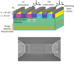
Interdigitated finger electrodes constitute a transmission metallic grating, which forms the top mirror of a Fabry-Perot resonator. The bottom mirror is a quarter-wave-stack multilayer Bragg reflector. The resonant cavity is made of a thin absorbing layer on top of a nonabsorbing spacing layer. The absorbing layer can be as thin as a few tens of nanometers; the thickness of the spacing layer is adjusted to satisfy the Fabry-Perot condition.
Transmission through the metallic grating occurs through a coupling of the incident wave with the optical modes into the slits. This coupling mechanism is different for TE and TM polarizations, resulting in different spatial distributions of the electric-field intensity (see Fig. 1). In TE polarization, the light is transmitted by a tunneling effect through the slits of the metallic grating, with the absorption region centered between the electrodes. In TM polarization, surface waves are involved in the transmission of light through the grating, resulting in enhanced absorption near the metal-semiconductor interfaces. The metallic grating acts as a high-reflectivity mirror for both polarizations, leading to an efficient coupling of the incident light with the cavity and an absorption efficiency of close to 100%.
We have fabricated these photodetectors on GaAs substrates with titanium/gold (Ti/Au) gratings and 100‑nm finger widths and finger spacings. Reflectivity and photocurrent measurements are in agreement with theoretical results. The TM-polarized resonance is very sensitive to the metal-semiconductor interface. The devices have reached an external quantum efficiency of 14% at an 810-nm wavelength in TE polarization, limited by fabrication technology. The agreement validates the theoretical approach and predicted performances: 75% external efficiency with a pure gold grating on top of a 24-period Bragg reflector should be achievable in an RCE SMSM photodetector.
Efficient light absorption
The RCE SMSM photodetector efficiently confines the absorption to a thin layer under subwavelength metallic electrodes; however, the electromagnetic properties of metallic nanostructures show potential for even more efficient and faster photodetection.
An efficient and ultrafast photodetector can be conceived as a nanoscale absorbing region between two closely spaced electrodes, yielding high quantum efficiency (greater than 50%) and high cut-off frequency (higher than 300 GHz). This approach is unrealistic in conventional photodetectors because of the absorption length in bulk semiconductors and the diffraction limit.
In a nanoscale MSM grating, however, the strong confinement of light between metallic wires resulting from Fabry-Perot-like resonances should, in principle, permit theoretical quantum efficiencies close to 75%. Moreover, the efficient collection of photocarriers through a high and homogeneous electric field with 50-nm mean collection path should allow theoretical cut-off frequencies as high as 500 GHz. Such a device is composed of a metal-semiconductor grating on a nonabsorbing spacing layer and a multilayer Bragg reflector. Metallic wires are connected to form interdigitated electrodes.
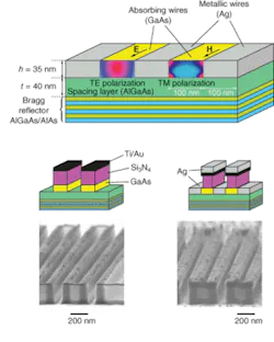
In TM polarization, the incident light is coupled to vertical surface-plasmon resonance in the slits for an appropriate grating height, leading to a huge confinement of light along the vertical metal-semiconductor interfaces (see Fig. 2). In TE polarization, the whole Fabry-Perot cavity is delimited by the grating-air interface as the upper mirror and a multilayer Bragg reflector as the lower mirror; most of the absorption is achieved in the center of the wire.
We fabricated metallic nanowires embedded in a GaAs layer by using a lift-off technique. The semiconductor layer structure is grown by molecular-beam epitaxy on a semi-insulating GaAs substrate. The aluminum arsenide/aluminum gallium arsenide (AlAs/AlGaAs) multilayer Bragg reflector is composed of 16 periods of quarter-wave AlAs/Al0.2Ga0.8As layers (67- and 57-nm height, respectively). The Al0.35Ga0.65As spacing and GaAs absorption layers are 59 and 40 nm thick, respectively. A 150-nm-thick layer of silicon nitride (Si3N4) was deposited on the sample by plasma-enhanced chemical-vapor deposition. The grating was defined by electron-beam lithography in a 100-nm-thick layer of polymethylmetacrylate. After resist development, Ti/Au (10/40 nm) layers were deposited by electron-beam-assisted evaporation and lifted off in trichloroethylene. The Si3N4 and GaAs layers were etched off using anisotropic reactive-ion etching (RIE). An overhang of the Ti/Au mask was then achieved by a light isotropic RIE and is subsequently followed by a 40-nm silver deposition on the sample surface. The nitride and metallic layers were lifted off by chemical etching. The resulting structure is a rectangular silver grating buried in an absorbing GaAs layer.
The reflectivity of 10 × 10-µm2 devices was measured in TM and TE polarizations. The roughness of the vertical metal-semiconductor interfaces of the grating induces additional absorption and diffusion effects that have been taken into account in the electromagnetic calculation of the structures. We found the results to be in very good agreement with the experimental data, and confirm the resonance mechanisms discussed previously. They highlight the importance of having high-quality vertical metal-semiconductor interfaces, especially for TM polarization.
Photocurrent measurements were performed on a device having a TE polarization resonance at a 780-nm wavelength; a 9% maximum external quantum efficiency was obtained in GaAs wires with cross sections as small as 40 × 100 nm2. From the carrier-transport point of view, a mean collection path of about 50 nm for photocarriers can be expected from the circular shape of the absorption region. This absorption is achieved in a region with a high and homogeneous electric field. With this geometry, the 500-GHz frequency range becomes realistic in a photodetector with theoretical efficiencies up to 75%. We strongly believe these results will help realize highly efficient and ultrafast photodetectors.❏
REFERENCES
1. S. Collin, F. Pardo, and J.-L. Pelouard, Appl. Phys. Lett. 83, 1521 (2003),
2. S. Collin, F. Pardo, R. Teissier and J.-L. Pelouard, Appl. Phys. Lett. 85, 194 (2004).
STÉPHANE COLLIN is a researcher at the Laboratoire de Photonique et de Nanostructures (CNRS/LPN), Route de Nozay, 91460 Marcoussis, France; e-mail: [email protected].


