PHOTODIODES- Resonant-tunneling detector counts photons

While crucial for quantum-cryptographic systems, single-photon detectors have other uses that extend from medical diagnosis to laser ranging. Avalanche photodiodes and photomultiplier tubes work as photon counters; however, their avalanche-multiplication schemes, which provide only indirect detection of single photons, can have associated problems. Trapped carriers in avalanche photodiodes, for example, limit the maximum data-transmission rate of quantum-cryptographic systems.
Researchers at Toshiba Research Europe and the University of Cambridge (both of Cambridge, England) have now developed a quantum-dot detector that directly senses single-photon-excited carriers, allowing low-noise detection.1 In the device, a single-photon-produced hole in a layer of quantum dots causes a change in the resonant tunnel current passing through an adjacent double-barrier structure.
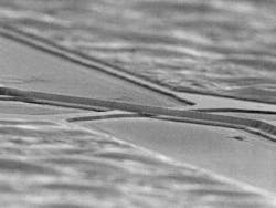
The gallium arsenide (GaAs)-based semiconductor-diode device contains a GaAs intrinsic region with a double-barrier tunnel structure adjacent to a layer of indium arsenide quantum dots populated to a density of about 100/µm2. To achieve a small tunnel-junction area, a cross-wire geometry was fabricated by etching two semiconductor wires such that the top wire was freestanding except for a 1-µm-square contact between the wires (see figure). For experimental comparison, large-area (with sides of 5 to 50 µm) devices were also fabricated.
While the large-area structures showed a steady increase in tunnel current upon illumination, the smaller-area devices showed abrupt discrete steps. Each step, the researchers believe, is the result of a charging or discharging of a single quantum dot responding to a photon-produced hole. A monochromatic attenuated source of 550-nm light producing a known rate of photons allowed the researchers to measure quantum efficiency, which reached about 11% for the particular setup. A compromise can be made between the dark-count rate and the detection efficiency—a 12.5% efficiency for a dark-count rate of 2 × 10⁻³ s-1 (about one dark count every ten minutes), and 5% for a dark-count rate of 3 × 10⁻⁴ s-1 (about one dark count per hour).
Thinner is faster
The thickness of the barrier layers determines the magnitude of the tunnel current, with the strength of the single-photon signal greatly increased by the use of thinner barriers (3 vs. 10 nm). “The barrier thickness essentially determines the speed of the device,” notes Andrew Shields, a Toshiba researcher. “The device with 10-nm barriers is good for measuring photon fluxes for which the average time separation between photons is several seconds, while the 3-nm barrier sample is useful for measuring photons with microsecond separation times.”
The device is most sensitive to wavelengths between 400 and 820 nm. Adding high-bandwidth differentiating electronics converts each rapidly occurring step into a pulse, allowing photons to be counted with conventional electronics. The transient response of the detector to a periodic train of 684-nm laser pulses was measured, showing a jitter of about 150 ns—low enough to enable measurement of single-photon pulses arriving at a rate of 5 MHz.
The sensor is well suited for quantum cryptography, which has typical count rates of 10-3 to 10-5 per clock cycle. With improvement, the detector may find use in medical imaging and diagnosis, chemical analysis, atmospheric monitoring, scientific research, and fiberoptic strain and temperature sensors.
REFERENCE
1. J. C. Blakesley et al., Phys. Rev. Lett. 94, 067401 (Feb. 18, 2005).
About the Author
John Wallace
Senior Technical Editor (1998-2022)
John Wallace was with Laser Focus World for nearly 25 years, retiring in late June 2022. He obtained a bachelor's degree in mechanical engineering and physics at Rutgers University and a master's in optical engineering at the University of Rochester. Before becoming an editor, John worked as an engineer at RCA, Exxon, Eastman Kodak, and GCA Corporation.
