Photomultiplier tubes are at the forefront of low-light detection
For low-light detection, photomultiplier tubes (PMTs) have always provided high sensitivity and low noise. PMTs have newer competitors in the form of silicon photomultipliers (SiPMs), avalanche photodiodes (APDs), and single-photon avalanche photodiodes (SPADs)—however, the PMT has qualities that make it the choice for numerous low-light applications. While this article cannot include more than a small portion of the available PMT products, a representative sampling of what can be found is presented here.
What’s in a PMT
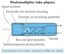
As described by Slawomir Piatek, science consultant for Hamamatsu (Hamamatsu City, Japan), a PMT is a light-sensitive, cold vacuum tube with three main components. First is the photocathode, where the incident photon is absorbed, leading to a possible emission of an electron into vacuum (the photoelectric effect). Second, an arrangement of dynodes together is responsible for the intrinsic gain of a PMT. The electron emitted from the photocathode is accelerated by the internal electric field towards the first dynode. It strikes the dynode as the primary electron, shares its energy with some internal to the dynode electrons, and some fraction of these electrons, called secondary electrons, escapes into vacuum. Once the secondary electrons from the first dynode escape into vacuum, they are accelerated towards the second dynode, become primary electrons to that dynode, and the second dynode releases even more secondary electrons. This chain of acceleration and emission is repeated at every dynode. Last, the anode collects electrons emitted from the final dynode and allows them to flow to the “outside world” for electronic processing.
“Roughly, the family of PMTs can be divided into two groups based on how the incident photon interacts with the photocathode,” adds Earl Hergert, Hamamatsu’s vice president of marketing. “In a head-on, or semitransparent model, an incident photon and the emitted photoelectron are always on the opposite sides of the photocathode, whereas in a side-on or opaque model, both the incident photon and the emitted photoelectron are always on the same side.”
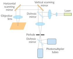
The intrinsic gain of a PMT is very high, ranging from less than 105 to more than 107. Such high gain makes a photodetector sensitive to very low light levels, and even to a single photon. PMTs are found in such applications as neutrino and dark-matter detectors in high-energy physics; flow cytometry in biology and medicine; long-range spectroscopic lidar in environmental science; hygiene monitors for food safety; and confocal, two- and three-photon, and other forms of microscopy in biology and medicine (see Fig. 1).
There are literally several dozens of PMTs to select from, notes Hergert. “As often is the case, some models are more popular because of their fit-all characteristics: the R3896 side-on PMT is such model produced by Hamamatsu. Its spectral response ranges from about 200 to 900 nm using a multialkali photocathode. The size of the photocathode is an 8 × 24 mm rectangle. Nine dynodes are arranged in a circular cage. The PMT requires a bias voltage of about 1250 V, which results in a cathode-to-anode gain of 107.
Flow cytometry, a technique of studying, counting, and sorting microcells, offers a case study where all four cardinal point detectors—photodiode, APD, SiPM, and PMT—are used in the photodetection section of a flow cytometer, says Piatek. A modern flow cytometer can have dozens of optical channels per single cell detection. Each channel is terminated with a photodetector. The choice of the photodetector per channel depends on the wavelength, incident power, and time characteristics of the incident light. In the forward-scatter channel, there is usually enough light to warrant the use of a photodiode. However, in the side-scatter channel and, especially, in fluorescence channels, the incident light powers are low, necessitating the use of a photodetector with the intrinsic gain.
Of the three photodetectors with the intrinsic gain, PMT has the highest and, at the same time, one that can be varied by orders of magnitude. The gain of an SiPM is on the order of 105 to 106, but cannot be changed without adversely affecting the performance of the detector. In the case of a linear-mode APD, the useful gain is up to about 100.
The intrinsic gain of a photodetector comes with a noise penalty, Piatek explains. The multiplication noise is expressed with an excess noise factor F, which is 1 for an ideal case (noiseless multiplication) and greater than 1 for nonideal. The larger it is, the greater amount of noise is introduced by the gain mechanism. The excess noise factor for PMTs and SiPMs is comparably low and on the order of 1.1 to 1.2, whereas for linear-mode APDs, it is higher—in the 3 to 4 range. Multiplication noise results from a gain variation, which introduces detector-induced scatter in the archetypal scatter plots and histograms of flow cytometry.
Some channels in a flow cytometer require the photodetector to have wide dynamic range, or the ability to detect a range of light signals from weak to intense. The photodetector’s dark current limits its ability to detect weak light signals, whereas saturation effects limit the detection of more intense signals. Of the three photodetectors with gain, PMT has the smallest dark current per unit active area, and, therefore, has the greatest sensitivity. In contrast, it takes the highest input light level to saturate an APD. Saturation level of a SiPM is controlled by its number of its microcells. A side-by-side comparison between a PMT and SiPM would show that it takes less incident light to saturate a SiPM than a PMT. It’s worth noting that the dynamic range of a PMT can be controlled with a bias voltage and also with the voltage-divider circuit. This allows a “dynamic range window” to be moved up or down in a PMT, but not in a SiPM.
Resellers, too
A number of well-known optical-component providers resell PMTs made by large PMT manufacturers. For example, Oriel, a brand of Newport (Irvine, CA), purchases them from Hamamatsu, according to John Park, applications engineering manager at Newport (which is itself owned by MKS Instruments). “However, Oriel manufactures the PMT power supply, detector housing, and accessories to complete the system for customers,” notes Park, who adds that photomultipliers are more sensitive than any other detector in the near-UV and visible regions. The company offers end-on (see Fig. 2) as well as side-on models.“Our side-on tubes have similar components arranged in a much tighter geometry, which makes packaging easier and removes some of the environmental sensitivities of these superb detectors,” says Park. “The end-on tubes have larger and more uniform photosensitive areas; side-on tubes have faster rise times and reach higher responsivities, since most of them use opaque photocathodes, thus avoiding the optical losses associated with the semitransparent photocathodes of the end-on tubes. Primary use of our PMTs is in apps where noise-equivalent power is as low as possible. Examples of these apps include single-photon microscopy, material characterization, and other single-photon-detection experiments.”
Park says that the Oriel 77348 PMT is the company’s most popular device, due to its broad spectral range from the UV to near-infrared (near-IR). The detector also has low noise-equivalent power (NEP), with a rated specification of 1.2 × 10⁻¹⁶ W-Hz-1/2. Its high peak responsivity results in a large amplified signal per incident photon, making the PMT ideal for very low light conditions, notes Park. “A popular application for this PMT includes single-photon microscopy, because it requires extremely low noise and light while delivering significant current amplification,” he adds. “The optional PMT housing ensures a secure fit with Oriel monochromators, eliminating undesired stray light.”
Microchannel-plate PMTs
Another form of PMT, one with high bandwidth and immunity to magnetic fields, is the microchannel-plate (MCP) PMT, says James Milnes, research and development manager at Photek (St. Leonards-on-Sea, England), a company that specializes in these devices. Composed almost entirely of glass, metal, and ceramic, MCP-PMTs are also very resistant to radiation damage. These characteristics enable MCP-PMTs to be used in environmentally demanding applications such as plasma diagnostics, high-energy and nuclear physics, and space. Their combination of excellent temporal response and very low noise are also used in advanced analytical instrumentation for time-correlated single-photon counting and time-resolved spectroscopy.
Photek’s MCP-PMTs have spectral sensitivity from the vacuum-UV to near-IR, says Milnes, and have exceptional analog bandwidth up to 5 GHz and immunity to magnetic fields up to 2 Tesla. Configurations include single anode MCP-PMTs with active areas of 10, 25, and 40 mm, and multi-anode MCP-PMTs with form factors of 40 mm diameter and 59 mm square having anode pitch as small as 0.828 mm. Depending on the application, one, two or three MCPs can be used to provide gain of up to 107.
As an example, Milnes selects the AuraTek MAPMT253, which has an active area of 53 mm square and was developed originally for the TORCH time-of-flight detector proposed for the Large Hadron Collider beauty (LHCb) experiment upgrade at CERN near Geneva, Switzerland. “The detector was chosen over alternatives such as SiPM due to its superior single-photon time resolution of 30 ps, higher spatial resolution, and orders-of-magnitude lower dark counts of roughly 2 cps/channel,” says Milnes. “To achieve spatial resolution of at least 400 µm in one dimension, a patented segmented anode was used. The anode’s 8 × 64 segments have pitch of 6.624 and 0.828 mm, respectively. The anode pads are strategically placed inside the ceramic anode to create charge sharing between adjacent anode segments. Interpolation of this charge sharing provides spatial resolution of about 0.1 mm along the 64 anode dimension, better than required and with fewer required readout channels.” Photek also designed the device to meet the 5- to 10-year lifetime requirement at high operational signal levels, Milnes adds.
Hybrid modules
PMTs can be combined with other single-photon-detection technologies, too. HORIBA Scientific (Piscataway, NJ) manufactures a range of single-photon-detection modules containing both PMT and APD technology. “These are designed to simplify the use of PMTs for photon-counting applications and are especially suited to time-resolved photon counting in the picosecond and nanosecond regimes,” says David McLoskey, managing director at HORIBA. “Typical applications of such modules include ultrasensitive spectroscopy and time-of-flight measurements such as lidar, tomography, and time-correlated single-photon counting (TCSPC), where timing fidelity cannot be compromised.”
The basic purpose of the detection module is to detect and convert the incident photon into a logic pulse for connection to signal processing electronics, such as a simple counter or a time-to-digital converter (TDC). “HORIBA’s modules are unique in that they contain all of the electronic building blocks required for high-time-resolution counting: PMT, thermoelectric control, high-voltage (HV) bias, amplifier, and, crucially, the constant-fraction type discriminator that marks the transition of the signal from the analog to the digital domain,” notes McLoskey. “Conversion to digital logic (such as TTL) inside the PMT housing greatly simplifies the operation of the PMT, since there are no RF or electromagnetic-immunity issues to deal with. Furthermore, all settings are optimized in the factory so that the learning curve for the operator could not be shorter.”
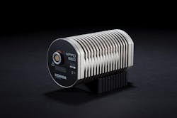
The company recently introduced a new range of detection modules based on hybrid PMTs, which McLoskey says combine the advantages of classic vacuum-tube technology, such as wide spectral response (from UV to near-IR) and large active area, with the fast timing characteristics often associated with small-active-area APDs or SPADs. Despite their performance advantages, however, hybrid PMTs in their discrete form are even more complicated to use than normal PMTs for three reasons, McLoskey explains. First, they require two separate HV bias supplies, one for the APD and one for the vacuum tube. Second, the photomultiplication is relatively low, resulting in millivolt signals that are vulnerable to noise pickup. Third, the APD stage has a strong temperature dependence, meaning that temperature control of the device is mandatory for timing applications. But, by adopting the design philosophy used in HORIBA’s other detection modules, the company’s hybrid picosecond photon detection modules (HPPDs) resolve all of these complications in a package that is simple and robust, explains McLoskey.HORIBA now makes use of its HPPD-860 hybrid module (see Fig. 3) in its optical test lab, where its different types of picosecond-pulse laser diodes are calibrated and tested. After using a MCP-PMT for this purpose, the company moved to the HPPD-860 because, as McLoskey says, MCP-PMTs are easily damaged by accidental over-illumination and also exhibit an afterpulse artifact on the nanosecond time scale. “The HPPD has the same time resolution as the MCP-PMT, but it can tolerate a much greater incident photon flux, which makes it more flexible in a lab environment,” he says. “Furthermore, it is almost entirely free of afterpulsing artifacts, which enables a closer inspection of the shape of our picosecond laser pulses.”
For More Information
Companies mentioned in this article include:
Hamamatsu
Hamamatsu City, Japan
HORIBA Scientific
Piscataway, NJ
Newport Oriel
Irvine, CA
www.newport.com/b/oriel-instruments
Photek
St. Leonards-on-Sea, England
DISCLAIMER: While we try to include information from the broadest possible number of companies that manufacture the products featured in our Photonics Products series, because of limited word count as well as deadlines that cannot always be met by requested contributors, we cannot possibly include all companies and regret if your company is not included in our series.
About the Author
John Wallace
Senior Technical Editor (1998-2022)
John Wallace was with Laser Focus World for nearly 25 years, retiring in late June 2022. He obtained a bachelor's degree in mechanical engineering and physics at Rutgers University and a master's in optical engineering at the University of Rochester. Before becoming an editor, John worked as an engineer at RCA, Exxon, Eastman Kodak, and GCA Corporation.


