The photodiode retains its status as the basic solid-state detector. This fundamental device is the springboard for more specific forms, such as the avalanche photodiode with its built-in amplification. More developments can be expected, with current research efforts branching in three main directions—photodiodes are being integrated into fiberoptic receivers that operate at higher and higher data rates, special-purpose photodiodes are emerging that isolate sharply defined parts of the spectrum for observation, and polymer photodiodes are beginning to offer higher efficiency at increasingly lower costs.
Photodiodes consist of a material layer doped with atoms carrying one valence electron less than neutral (p-type semiconductors) that resides on top of a layer doped with atoms carrying extra valence electrons (n-type semiconductor). Charge migration creates a depletion region with an electric field directed toward the p-region, allowing current to flow in only one direction. Apply a reverse bias potential across the diode, and in the absence of light, only a dark current due to thermal generation of electrons is present. Light exposure creates electron-hole pairs, generating a current.
Upping the speed
One of the most intense areas of photodiode development is the never-ending pursuit of high-speed receivers for fiberoptic communications systems. One current technical trend involves the monolithic integration of photodiodes and transistors onto a single chip. Another trend is the development of new types of photodiodes as parts of these optoelectronic integrated circuits (OEICs).
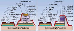
For fiberoptic applications, photodiodes are generally made using indium gallium arsenide (InGaAs), which has good absorption properties in the 1.55-µm band. A conventional p-i-n design has an InGaAs layer between p- and n-doped layers of indium phosphate (InP). These materials allow researchers to build a high-electron mobility transistor (HEMT) onto the same chip (see Fig. 1).
One variation of this conventional design is the waveguide photodiode (WGPD), which creates a waveguide so that light enters the detector from the side, instead of above or below. The advantage is that the light can travel through a greater thickness of absorbing material without requiring a larger vertical thickness of the layer.
With a thin photo-absorbing layer, however, the electrons and holes still must travel short distances to enter the electrode. While response time does not increase, sensitivity does. Side illumination also makes it easier to interface with planar lightwave circuits that feed the light horizontally. The key to the WGPD design is a highly doped intermediate InGaAs layer between the core layer and the InP cladding layers.
So how high are data transmission rates? In experiments performed at the NTT Photonics Laboratory (Atsugi, Japan), scientists obtained a frequency response as high as 46.5 GHz.1 While there is some dispute in the field as to what that translates into in terms of data transmission rates, the NTT team equates that specific frequency response to 40 Gbit/s.
Another design under development at the same laboratory is the unitraveling carrier-type photodiode.2 This approach attempts to circumvent the need for any electronic amplification at ultrahigh frequencies. Instead, the signal is optically amplified with erbium-doped fiber amplifiers before being fed to the detector.
With conventional detectors, electronic amplification at ultrahigh frequencies will lead to current saturation because the holes, which move relatively slowly, can't move as fast as the electrons. With the new type of photodiode, as the electron current builds, a positive space charge accumulates, eventually holding back the electrons and causing the current to saturate.
In the unitraveling carrier design, only the electrons carry the current. Incident light generates carriers in a p-type neutral absorption layer. The electrons, which diffuse quickly, are injected into the depleted carrier collection layer. This suppresses the buildup of the space charge and improves output. The photodetectors, operating independently, responded to levels as high as 152 GHz. When devices were mounted into a module to form an optical receiver, though, their performance dropped to around 40 GHz.
Another new type of high-speed photodiode is the dual-depletion p-i-n detector.3 This approach addresses another trade-off required for increased speeds. To get carriers to the electrodes faster, for instance, it seems logical to make the absorption layer thinner and the electrodes closer to each other. This move, however, increases the capacitance of the circuit (inversely proportional to the electrode spacing), which in turn slows the circuit response. Again, the holes are more of a problem relative to travel time because they move more slowly than the electrons and thus determine the total transit time.
The goal of the dual-depletion design now in development at Discovery Semiconductors (Princeton, NJ), among other research groups, is to generate the carriers as close as possible to the cathode of p contact, so that the holes will have a shorter distance to travel than the electrons. Two different compositions of semiconductor are used in the depletion region to achieve this goal—one layer that absorbs (InGaAs) and one that is transparent (InP). The carriers are generated only in the absorbing material, which is placed against the p contact. In this way the InP layer decreases capacitance without increasing transit time. The Discovery Semiconductors researchers report a 65-GHz response with their design.
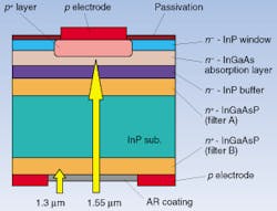
Another novel photodiode design is aimed at bidirectional optical transceiver modules, which receive and transmit optical signals at different wavelengths through a single optical fiber.4 To do so, however, optical crosstalk between the transmitting laser diode and the receiving photodiode must be minimized by narrowing the receiver waveband.
To design a photodiode that would be sensitive to 1.55-µm light and insensitive to 1.3-µm light, a research team at Sumitomo Industry (Yokohama and Osaka, Japan) used a double filter layer of InGaAsP in a rear-illuminated diode (see Fig. 2). While some holes generated by 1.3-µm radiation do leak in, there is a 28-dB suppression of the signal.Selecting wavelengths
Rapid progress is also being seen in photodiodes tailored to respond to specific wavelength bands, especially the ultraviolet (UV). Detectors that respond only to the UV, but are solar blind or at least visible blind, have a range of applications, including the capture of welding images, flame sensing, atmospheric ozone detection, astronomical sensing, and missile and shellfire detection. The trick is to engineer a very sharp long-wavelength cutoff, because visible light far overpowers UV radiation under solar illumination.
These photodiode designs are based on aluminum gallium nitride (AlGaN). With this wide band-gap material, it is possible to change the band gap and thus the absorption characteristics by altering the proportions of elements in the composition. In a solar-blind UV-sensitive photodiode designed by a research team from Cree Lighting Company (Goleta, CA) and the University of California, Santa Barbara (Santa Barbara, CA), a wide band gap, or short-wavelength layer of AlGaN is sandwiched between two narrow band-gap contact layers. This is the opposite of the conventional arrangement.5 In this inverted heterostructure photodiode (IHP), the top contact layer is sufficiently thin to minimize absorption of the UV photons. At the same time, the longer-wavelength photons that are absorbed in this layer produce their own electron-hole pairs. Because the high level of doping in the layer allows for rapid recombination, the charge carriers can't make it out of the layer.
In the active layer, only the UV photons with energy above the band gap will be absorbed and produce a signal. In addition, a sufficient difference between the gaps in the active and adjoining layers will prevent carriers from moving into the active layer. For both front- and back-illuminated versions of this design, the drop in sensitivity between 285 and 325 nm is more than a factor of 1000.
Using a somewhat different approach, a research team, including scientists from North Carolina State University (Raleigh, NC), the Night Vision and Electronic Sensors Directorate (Fort Belvoir, VA), and Honeywell Technology Center (Plymouth, MN), has developed designs with higher-wavelength windows. One of the devices is sensitive from 285 to 320 nm, another from 320 to 358 nm.6
Exploring plastic diodes
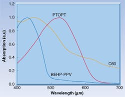
Also of current interest to researchers are improved polymer photodiodes, which have the potential to increase the efficiency of both photodiodes and solar energy cells and decrease their cost. A wide variety of polymers are currently being used and studied. A typical example is the extended-spectral-coverage photodiode under development at Linköping University (Linköping, Sweden) and the Chalmers University of Technology (Goeborg, Sweden).7In this project, the goal is to combine several polymers to cover a broader range of wavelengths and boost overall quantum efficiency. The photodiode is fabricated from a polymer electrode of highly doped PEDOT-PSS with a donor layer of PTOPT and BEHP-PPV. An additional layer of fullerene is added to improve absorption in the red and near-infrared wavelengths (see Fig. 3). By changing the relative thickness of the three polymer layers, the team was able to fabricate photodiodes with spectral sensitivities tailored to extend far into the red or to be cut off at intermediate wavelengths, depending on the application requirements. They obtained peak quantum efficiencies as high as 35%. In the future, manufacturers may be able to produce such plastic photodiodes extremely cheaply, instead of with the expensive photolithography techniques used today.
REFERENCES
- K. Takahata et al., IEICE Trans. Elect. E83-C, 950 (June 2000).
- Y. Matsuoka and T. Ishibashi, OFC Proc. 37, 251 (October 2000).
- A. M. Joshi, Mat. Res. Soc. Symp. Proc. 607, 115 (November 2000).
- Y. Iguchi et al., Proc., 2000 Int. Conf. on Indium Phosphide and Related Materials, 317 (September 2000).
- E. J. Taresa et al., Appl. Phys. Lett. 77, 316 (July 2000).
- J. D. Brown et al., Mat. Res. Soc. Symp. Proc. 595, W1.9.1 (June 2000).
- L. C. Chen et al., Thin Solid Films 363, 286 (August 2000).
About the Author
Eric J. Lerner
Contributing Editor, Laser Focus World
Eric J. Lerner is a contributing editor for Laser Focus World.


