Uncooled IR detectors move into the mainstream
Although infrared (IR) detectors that require no cooling were introduced less than six years ago, they already have become a proven technology. Not only have the microbolometers that first made uncooled IR possible become more sophisticated and flexible, but progress is being made toward the challenging task of creating uncooled semiconductor detectors. Success would mean considerably higher speeds and sensitivities.
Infrared detectors come in two basic varieties—photon detectors, which produce electric currents in direct response to photons, and thermal detectors, or bolometers, which measure the total energy absorbed by a change in the temperature of the detector elements. If any object is thermally isolated—not allowed to conduct heat to its surroundings—any increase in absorbed radiation produces an increase in emitted radiation. Temperature also must rise. Bolometers use the simple physical principal that electrical resistance varies with temperature. Measuring changes in that resistance thus measures incoming radiation.
At room temperature, a radiation intensity of only 1 mW/cm2 will lead, at equilibrium, to an increase in temperature of 1 K. One-tenth of that change in temperature produces an easily detectable change in resistance, making bolometers quite sensitive. There also is no need to cool them to low temperatures.
Even with these features, until the mid-1990s, many considered the slow response time of bolometers to be a disadvantage since a device had to absorb enough heat to reach equilibrium before an accurate measurement could be made. Manufacturers resolved this issue with miniaturization, which only became possible with advances in micromachining processes based on silicon processing techniques. Since response time is proportional to the thickness of the absorber, for a thickness of about 0.5 µm, response times drop to tens of milliseconds. This is fast enough for normal video camera operation at 30 frames per second.
Microbolometer arrays
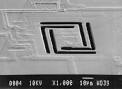
In a typical microbolometer array, material is etched away from around and under a 50-µm-square absorbing element, which in turn is supported by two electrical conductors, each only 0.1 µm thick and 5 µm wide (see Fig. 1). To isolate the element from underneath during fabrication, researchers use a sacrificial layer of polyimide, which ultimately dissolves away to free it. Thermal conduction through the tiny electrical conductors, which also serve as mechanical supports, is small enough that thermal sensitivities are within a factor of four of the theoretical maximum for a perfectly isolated device.
During the fabrication process, a thin aluminum layer is generally inserted underneath the absorbing element or microbridge to reflect the IR back up into it. The element itself combines a very thin layer of titanium nitride to absorb the IR radiaton with a 0.1-µm layer of amorphous silicon that acts as the thermometer. The individual microbolometers are formed as part of a square array of typically 256 × 256 pixels. A single silicon wafer can hold 12 such arrays. Since ordinary silicon and integrated circuit materials and processing techniques are used, yields are relatively high, and the costs of production are far lower than for quantum thermal arrays.
Within each bolometer, the absorbent material separates the conductors from each other. This is done by putting the conductor on opposite sides of the absorber, forming a gap design, or by locating one conductor on top and the other underneath the absorber to form a sandwich or a combined sandwich gap. By tailoring the thickness of the absorbing material, typically lightly doped silicon, the device manufacturers ensure that it combines high absorption in the mid-IR band around 10 µm with fast response time and good resistivity characteristics.
In addition to silicon, companies currently use a number of other materials, including barium strontium titanium oxide, titanium, and vanadium oxide in the fabrication process. The resulting bolometers are highly sensitive, capable of detecting temperature differences of 0.07 K with output response of about 10 mV/K. Uncooled microbolometer arrays are now widely available in commercial imaging cameras, although they remain fairly expensive, with prices typically in the area of $12,000.
Avoiding calibration
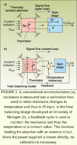
While uncooled IR detector technology has moved into commercial production, the devices have sensitivities that are highly process dependent and require elaborate calibration procedures and corrective electronics. To avoid these problems, researchers have been developing a heat-balancing approach using electrothermal feedback. Here, instead of directly detecting the temperature change by measuring changes in resistance, electric power is delivered to each detector pixel to balance the heat absorbed from the target and to maintain a constant resistance and thus constant temperature.
As incoming radiation increases, the power needed to maintain a constant temperature decreases. This power difference can be measured directly in terms of current supplied at a given voltage. Since the incoming power is the same as the difference in feedback power, no calibration is needed.
A research team at the University of Michigan's Center for Integrated Microsystems (Ann Arbor, MI) has demonstrated such a heat balancing detector using an 8 × 8 array fabricated with a commercial complementary metal oxide semiconductor (CMOS) process.1 The scientists obtained a sensitivity of about 1 MV/W, within a factor of 10 of the best microbolometer sensitivity, but without the complex calibration required by conventional approaches (see Fig. 2). Considerable development work is still necessary to produce a high-resolution heat-balancing array.HOT Photonic arrays
The alternative to bolometers is photonic detectors, in which photons produce free charges that are collected as a current. For the IR band, mercury cadmium telluride is the primary material. The problem with these detectors is that the dark current, the flow of current produced by thermal processes when there is no incoming IR, increases as temperature rises. For medium-wavelength IR (MWIR), cooling to below 180 K is necessary. For long wavelength IR (LWIR), devices must be cooled below 120 K.
In the past few years, research has intensified into a possible solution called high operating temperature or HOT processing. First proposed back in 1985, this approach uses a narrow-gap layer sandwiched between two wider-gap materials in the case of mercury cadmium telluride, or between a wider gap material and a heavily doped layer when using indium antinomide.2 The structure has a reversed-bias p-n junction that extracts the minority charge carriers.
This structure reduces dark current in several ways. First, the wide-gap regions have very low thermal generation rates. They also isolate the active region of the device from carrier generation at the contacts. The device's main advantage, though, is that, by sweeping out the minority carriers, the electrons, it directly reduces the leakage currents.
For years, the noise levels associated with these devices remained too high for imaging applications or for applications requiring room-temperature operation, but recent work at the Defense Research and Evaluation Agency (Malvern, England) and Marconi Infrared Ltd. (Southampton, England) indicates that further reductions in dark currents could lead to practical operation of the devices at 240 K, which is within the reach of thermoelectric coolers. This is not uncooled operation, but it is getting close.
In these devices, internal radiation mechanisms are important. Recombination of holes and electrons produces photons, which are then absorbed in the active region, generating a dark current. To reduce this current, the British researchers used a strange property of the device called negative luminosity, which is a reduction of the emission from a surface below the level needed to maintain thermal equilibrium. In other words, the body becomes blacker than a blackbody at the same temperature.
In equilibrium, the absorption of photons and the production of electron-hole pairs are balanced by electron-hole recombination and photon emission. Since the electrons are swept up so rapidly, though, they do not have time to recombine, and the entire active layer becomes a sink for photons, producing negative luminosity. This process reduces the dark current produced by intrinsic photon production.
While this work seems promising, for the time being microbolometer arrays are likely to remain the only commercialized uncooled IR detectors. As prices for these arrays drop, the cost of IR cameras will drop radically as well, enabling a rapid expansion of applications.
REFERENCES
- C.-C. Liu and C. H. Mastragelo, IEEE J. Solid State Circuits, 35, 527 (April, 2000).
- N. T. Gordon et al., J. Electronic Materials, 29, 818 (March, 2000).
About the Author
Eric J. Lerner
Contributing Editor, Laser Focus World
Eric J. Lerner is a contributing editor for Laser Focus World.

