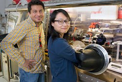
LANL technique grows near-18% efficient perovskite solar cells
Los Alamos National Laboratory (LANL; Los Alamos, NM) researchers describe a new solution-based hot-casting technique in the journal Science that allows growth of highly efficient and reproducible solar cells from large-area perovskite crystals. "These perovskite crystals offer promising routes for developing low-cost, solar-based, clean global energy solutions for the future," said Aditya Mohite, the Los Alamos scientist leading the project.
RELATED ARTICLE: A perovskite and AlGaN economy?
State-of-the-art photovoltaics using high-purity, large-area, wafer-scale single-crystalline semiconductors grown by sophisticated, high temperature crystal-growth processes are seen as the future of efficient solar technology. Solar cells composed of organic-inorganic perovskites offer efficiencies approaching that of silicon, but they have been plagued with some important deficiencies limiting their commercial viability. It is this failure that the Los Alamos technique successfully corrects.
The researchers fabricated planar solar cells from perovskite materials with large crystalline grains that had efficiencies approaching 18%, among the highest reported in the field of perovskite-based light-to-energy conversion devices. The cells demonstrate little cell-to-cell variability, resulting in devices showing hysteresis-free photovoltaic response, which had been a fundamental bottleneck for stable operation of perovskite devices.
"Characterization and modeling attribute the improved performance to reduced bulk defects and improved charge-carrier mobility in large-grain pervoskite materials," said Mohite, "and we've demonstrated that the crystalline quality is on par with that observed for high-quality semiconductors like silicon and gallium arsenides."
The researchers anticipate that their crystal growth technique will lead the field towards synthesis of wafer-scale crystalline perovskites necessary for the fabrication of high-efficiency solar-cells and be applicable to several other material systems plagued by polydispersity, defects and grain boundary recombination in solution-processed thin-films.
The work at Los Alamos National Laboratory was supported by a DOE Office of Basic Energy Sciences proposal and by the Los Alamos National Laboratory Directed Research and Development (LDRD) program. This work was done in part at the Center for Integrated Nanotechnologies, a DOE Office of Science User Facility. Researchers include Wanyi Nie, Hsinhan Tsai, Jean-Christophe Blancon, Amanda J. Neukirch, Gautam Gupta, Jared J. Crochet, Sergei Tretiak, Hsing-Lin Wang and Aditya D. Mohite of Los Alamos, in addition to Reza Asadpour (Purdue University), Manish Chhowalla (Rutgers Univesity) and Muhammad A. Alam (Purdue University).
SOURCE: LANL; http://www.lanl.gov/discover/news-release-archive/2015/January/01.29-high-efficiency-perovskite-solar-cells.php

Gail Overton | Senior Editor (2004-2020)
Gail has more than 30 years of engineering, marketing, product management, and editorial experience in the photonics and optical communications industry. Before joining the staff at Laser Focus World in 2004, she held many product management and product marketing roles in the fiber-optics industry, most notably at Hughes (El Segundo, CA), GTE Labs (Waltham, MA), Corning (Corning, NY), Photon Kinetics (Beaverton, OR), and Newport Corporation (Irvine, CA). During her marketing career, Gail published articles in WDM Solutions and Sensors magazine and traveled internationally to conduct product and sales training. Gail received her BS degree in physics, with an emphasis in optics, from San Diego State University in San Diego, CA in May 1986.
