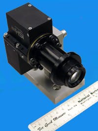
Corning buys NovaSol for its hyperspectral imaging capabilities
Corning Incorporated (NYSE: GLW; Corning, NY) has acquired the assets of NovaSol (Honolulu, HI), a maker of hyperspectral imaging systems. The terms of the agreement were not disclosed. NovaSol will be integrated into the Advanced Optics business unit within Corning’s Specialty Materials division.
Founded in 1998, NovaSol specializes in the R&D of active and passive optical systems, including electro-optical systems and optical communication systems. Corning says that NovaSol’s technology portfolio, combined with Corning’s expertise in the design, development, and manufacture of optical imaging systems, will deliver high-performance, low-cost solutions. In addition, Corning will be able to more efficiently address the needs of emerging industrial markets for advanced spectral imaging solutions.
NovaSol's line of microHSI sensors achieve a combination of size, weight, and power (SWaP) and high spatial and spectral performance with a miniaturized solid optical block spectrograph design, which embeds a low optical aberration Offner relay with integrated high efficiency diffraction grating into a solid glass block. Without air spacing, the light ray paths are highly condensed, resulting in the low SWaP and mechanical and thermal robustness.
Source: Corning Incorporated

Conard Holton
Conard Holton has 25 years of science and technology editing and writing experience. He was formerly a staff member and consultant for government agencies such as the New York State Energy Research and Development Authority and the International Atomic Energy Agency, and engineering companies such as Bechtel. He joined Laser Focus World in 1997 as senior editor, becoming editor in chief of WDM Solutions, which he founded in 1999. In 2003 he joined Vision Systems Design as editor in chief, while continuing as contributing editor at Laser Focus World. Conard became editor in chief of Laser Focus World in August 2011, a role in which he served through August 2018. He then served as Editor at Large for Laser Focus World and Co-Chair of the Lasers & Photonics Marketplace Seminar from August 2018 through January 2022. He received his B.A. from the University of Pennsylvania, with additional studies at the Colorado School of Mines and Medill School of Journalism at Northwestern University.
