Simpler high-efficiency Si solar cell needs no impurity doping, may cost less
Crystalline silicon (c-Si) photovoltaic cells are the most common solar cells on the market. All these cells use a process called impurity doping to properly route the photogenerated electrons and holes that create electrical current; however, impurity doping adds cost and in addition has qualities that could impede some efforts to increase the efficiency of c-Si cells.
Now, researchers from the U.S. Department of Energy’s Lawrence Berkeley National Laboratory (Berkeley Lab), University of California Berkeley, Australian National University (ANU; Canberra, Australia), and the Swiss Federal Institute of Technology of Lausanne (EPFL; Neuchâtel, Switzerland) have eliminated the need for impurity doping by applying a new mix of materials to a standard c-Si design.1
In impurity doping, the wafer itself, and sometimes the layers deposited on the wafer, are doped; in these devices, two types of dopant atoms are required at the solar cell’s electrical contacts to regulate how the electrons and holes travel in a solar cell so that sunlight is efficiently converted to electrical current that flows out of the cell.
Seven steps
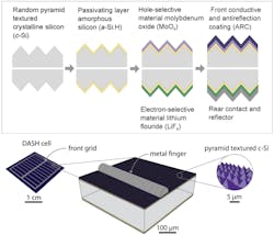
c-Si solar cells with doped contacts can exceed 20% efficiency, while dopant-free silicon cells had not previously exceeded 14% efficiency. The new study, though, demonstrated a dopant-free silicon cell—referred to as a dopant-free asymmetric heterocontact (DASH) cell—with an average efficiency above 19%. The increased efficiency is a product of the new materials and a simple coating process for layers on top and bottom of the device. The researchers showed that it is possible to create the new type of photovoltaic cell in just seven steps.
In the technique, layers of dopant-free amorphous silicon are applied to a crystalline silicon core; an ultrathin coatings of molybdenum oxide was applied to the sun-facing side of the solar cell and lithium fluoride to the bottom surface. The two layers, having thicknesses of tens of nanometers, act as dopant-free contacts for holes and electrons, respectively. Both materials are transparent, and they have complementary electronic structures that are well-suited for solar cells.
One of the Berkeley researchers, Ali Javey, notes that his group had discovered the utility of molybdenum oxide as an efficient hole contact for crystalline silicon solar cells a couple of years ago. “It has a lot of defects, and these defects are critical and important for the arising properties. These are good defects,” he says.
Source: https://newscenter.lbl.gov/2016/01/27/simplifying-solar/
REFERENCE:
1. James Bullock et al., Nature Energy, 25 January 2016; doi: 10.1038/nenergy.2015.31

John Wallace | Senior Technical Editor (1998-2022)
John Wallace was with Laser Focus World for nearly 25 years, retiring in late June 2022. He obtained a bachelor's degree in mechanical engineering and physics at Rutgers University and a master's in optical engineering at the University of Rochester. Before becoming an editor, John worked as an engineer at RCA, Exxon, Eastman Kodak, and GCA Corporation.
